


162 SA-1110 Developer’s Manual
Memory and PC-Card Control Module
If any of the DRAM require a full burst (all rows) CBR upon exiting self-refresh, the programmer
may use repeated single (nonburst) accesses to any disabled DRAM bank.
10.6 Static Memory Interface
The static memory interface is comprised of six chip selects, nCS[5:0]. nCS[2:0] are each
configurable for nonburst ROM or Flash memory, burst ROM or Flash, or SRAM. nCS[5:3] are
each configurable for nonburst ROM or Flash, burst ROM or Flash, or SRAM-like variable latency
I/O devices. The variable latency I/O interface differs from SRAM in that it allows the use of data
ready input signal, RDY, to force a variable number of memory cycle wait states. The data bus
width for each chip select region may be programmed to be 16-bit or 32-bit. nCS[3:0] are also
configurable for SMROM, but only for 32-bit data busses. nOE is asserted for all reads. nWE is
asserted for Flash and SRAM writes. For SRAM and variable latency I/O implementations,
nCAS/DQM[3:0] signals are used for the byte enables, where nCAS/DQM 3 corresponds to the
MSB. The SA-1110 supplies 26 bits of byte address (A[25:0]) for access of up to 64 Mbytes per
chip select. Address pin A 0 is not used in 16-bit wide bus systems and address pins A[1:0] are not
used in 32-bit wide systems.
The RT (ROM type) fields in the MSCx registers specify the type of memory: nonburst ROM or
Flash; nonburst ROM, SRAM, or variable latency I/O; burst-of-four ROM or Flash; or
burst-of-eight ROM or Flash. The RBW (ROM bus width) fields specify the bus width for the
memory space selected by nCS[5:0]. If a 16-bit bus width is specified, transactions take place
across data pins D[15:0]. The SMROM_EN pin and/or SMCNFG register must be used to
configure nCS[3:0] for SMROM.
The SA-1110’s static memory interface is intended for the interfacing of asynchronous types of
memory devices (i.e. memory devices utilizing nCS[5:0] and not utilizing SDCLK[2:0]). The static
memory interface does not support the interfacing of synchronous memory type devices to the
SA-1110 with the exception of SMROM type devices which are static type memories with a
synchronous interface; see Section 10.6.9 for details on SMROM interfacing. Table 10-10 provides
a comparison of supported static memory types.
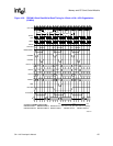
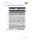
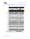
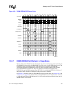
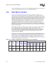
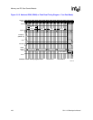
Table 10-10. Summary of Static Memory and Variable Latency I/O Capabilities
MSCx:
RT
Device
Type
Chip
Selects
Directions
Supported
for Single
Internal
Transfers
Directions
Supported
for Burst
Internal
Transfers
Timing (Memory Clocks)
Burst
Read
Address
Assert
nOE
Assert
Burst
nOE
De-
assert
Burst
Write
Address
Assert
nWE
Assert
Burst
nWE
De-
assert
00
Nonburst
ROM or
Flash
nCS[5:0]
Reads,
Writes
Reads RDF+1 RDF+1 0 N/A RDN+1 N/A
01
Nonburst
ROM or
SRAM
nCS[2:0]
Reads,
Writes
Reads,
Writes
RDF+1 RDF+1 0 RDN+2 RDN+1 1