


SA-1110 Developer’s Manual 169
Memory and PC-Card Control Module
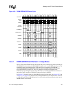
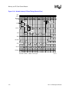
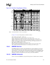
10.6.5 Variable Latency I/O Interface Overview
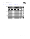
Variable latency I/O read accesses differ from SRAM read accesses in that nOE toggles for each
beat of a burst. The first nOE assertion occurs two memory cycles after the assertion of chip select
nCS 3, nCS 4, or nCS 5.
Both reads and writes differ from SRAM in that the SA-1110 starts sampling the data ready input
(RDY) at RDF-1 memory cycles after assertion of nOE or nWE: two (2) memory cycles prior to
end of minimum nOE or nWE assertion. Samples are taken every half memory cycle until three
consecutive samples (at rising, falling, and rising edges of the memory clock) indicate that the I/O
device is ready for data transfer. RDY can be tied high to cause a zero-wait-state I/O access. Read
data is latched one-half memory cycle after the third successful sample (on falling edge). nOE or
nWE is deasserted on the next rising edge and the address may change on the subsequent falling
edge. Prior to a subsequent data beat, nOE or nWE will remain deasserted for RDN+1 memory
cycles. The chip select and byte selects, nCAS/DQM[3:0], will remain asserted for one memory
cycle after the burst’s final nOE or nWE deassertion.
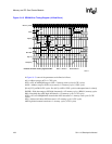
A single CBR refresh cycle, for asynchronous DRAM and/or SDRAM, may be inserted between
word accesses within a burst transaction. nCS, nOE, and nWE are deasserted during the refresh
cycle. The DRAM refresh interval must be adjusted to account for the longest variable latency I/O
access time (see Section 10.3.2). Because the longest access time includes the maximum number of
wait cycles caused by deassertion of the RDY pin, indefinitely long deassertions will prevent
refresh and may corrupt the DRAM contents.
Note: Using SRAM with nCS[2:0] results in higher memory read access performance than using SRAM
with nCS[5:3] and RDY tied high, see Section 10.6.3 and refer to Figure 10-12 and Figure 10-14
timing diagrams to calculate performance difference.
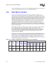
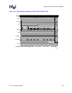
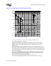
10.6.6 Variable Latency I/O Timing Diagrams and Parameters
Figure 10-14 shows the timing for variable latency I/O reads and Figure 10-15 shows the timing
for variable latency I/O writes.