


354 SA-1110 Developer’s Manual
Peripheral Control Module
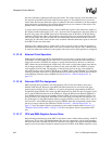
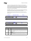
Note: A question mark (?) signifies that the Reset value of that bit is undefined when the processor has
completed its reset cycle.
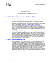
0h 8006 0000 MCP Control Register 0: MCCR0 Read/Write
31 30 29 28 27 26 25 24 23 22 21 20 19 18 17 16 15 14 13 12 11 10 9 8 7 6 5 4 3 2 1 0
Reserved ECP
LBM
ARE
ATE
TRE
TTE
ADM
ECS
MCE
Reserved
TSD
Reserved
ASD
Reset
0 0 0 0 0 0 0 0 ? ? ? ? ? ? ? 0 0 ? ? ? ? ? ? ? 0 ? ? ? ? ? ? ?
(Sheet 1 of 2)
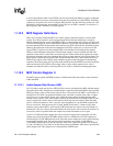
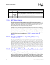
Bits Name Description
6..0 ASD
Audio sample rate divisor.
Value (from 4 to 127) used to match the sample rate of the audio codec within the
UCB1x00 to time when audio D/A data should be supplied by the audio transmit FIFO.
Sample Rate = Programmed clock rate/(32xASD), where ASD is a decimal value.
7 — Reserved.
14..8
Telecom sample rate divisor.
Value (from 4 to 127) used to match the sample rate of the telecom codec within the
UCB1x00 to time when telecom D/A data should be supplied by the telecom transmit FIFO.
Sample Rate = Programmed clock rate/(32xTSD), where TSD is a decimal value.
15 — Reserved.
16 MCE
Multimedia communications port enable.
0 – MCP operation disabled, control of the TXD4, RXD4, SCLK, and SFRM pins given to
the PPC to be used as general-purpose I/O pins.
1 – MCP operation enabled.
Note that the MCP has precedence over the SSP, if MCE=1; SSE is ignored unless the
SPR bit is set within the PPC, which allows the SSP to use GPIO pins while the MCP uses
serial port 4’s pin for transmission.
17 ECS
External clock select.
0 – on-chip clock used to produce the frame rate as further programmed by the CFS control
bit in MCCR1. It is also used to clock the audio and telecom sample rate counters.
1 – Clock input using GPIO pin 21 to select a frame rate that is an exact multiple of the
desired audio/telecom sample rate.
Frame Rate = Input Clock Frequency /(ECP x 32).
Sample Rate = Input Clock Frequency /(ECP x 32 x ASD or TSD).
18 ADM
A/D data sampling mode.
0 – Audio and telecom receive data is stored to their respective FIFOs whenever their receive
data valid bits are valid.
1– Audio and telecom receive data is stored when the receive data valid bit is set the first
time, and from that point on whenever the MCP’s audio and telecom sample rate counters
time out.
19 TTE
Telecom transmit FIFO interrupt enable.
0 – Telecom transmit FIFO half-full or less condition does not generate an interrupt (TTS bit
ignored).
1 – Telecom transmit FIFO half-full or less condition generates an interrupt (state of TTS
sent to interrupt controller).
20 TRE
Telecom receive FIFO interrupt enable.
0 – Telecom receive FIFO one- to two-thirds full or more condition does not generate an
interrupt (TRS bit ignored).
1 – Telecom receive FIFO one- to two-thirds full or more condition generates an interrupt
(state of TRS sent to interrupt controller).