


368 SA-1110 Developer’s Manual
Peripheral Control Module
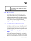
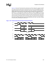
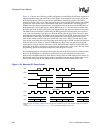
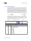
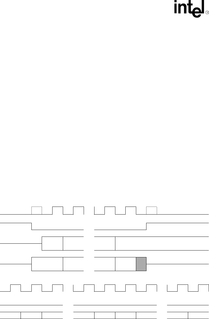
Figure 11-33 shows one of the four possible configurations for the Motorola SPI frame format for a
single transmitted frame and when back-to-back frames are transmitted. In this mode, SCLK and
the transmit data line (TXD4) are forced low and SFRM is forced high, whenever the SSP is
disabled or the SA-1110 is reset. Once the bottom entry of the transmit FIFO contains data, SFRM
is pulled low and remains low for the duration of the frame’s transmission. The falling edge of
SFRM causes the value for transmission to be transferred from the bottom transmit FIFO entry to
the transmit logic’s serial shift register, and the MSB of the 4- to 16-bit data frame is shifted onto
the TXD4 pin a half an SCLK period later (note that the SCLK pin does not transition at this point).
The MSB of the received data is shifted onto the RXD4 pin by the off-chip serial slave device as
soon as the serial framing signal goes low. Both the SSP and the off-chip serial slave device then
latch each data bit into their serial shifter on the rising edge of each SCLK. At the end of the frame,
the SFRM pin is pulled high one SCLK period after the last bit has been latched in the receive
serial shifter, which causes the data to be transferred to the receive FIFO. Note that the off-chip
slave device can tri-state the receive line either on the falling edge of SCLK after the LSB has been
latched by the receive shifter or when the SFRM pin goes high. Also note that the transmit pin
retains the last value it transmits (the value of bit 0, when the frame completes and the SSP enters
idle mode). If the SSP is disabled or a reset occurs, the transmit pin is reset to zero. All four frame
programming options are described in the SSP Control Register 1 section.
For continuous transfers, data transmission begins and ends in the same manner as a single transfer;
however, the SFRM line is continuously asserted (held low) and transmission of data occurs
back-to-back (the MSB of the next frame follows directly after the LSB of the previous frame). In
this example, each of the received data values is transferred from the receive shifter to the receive
FIFO on the falling edge SCLK after the LSB of the frame has been latched into the SSP.
Figure 11-33. Motorola SPI Frame Format
SCLK
...
SFRM
...
TXD4 BitN BitN..1 ... Bit1 Bit0
RXD4 BitN BitN..1 ... Bit1 Bit0
MSB 4 to 16 Bits LSB
Single Transfer
SCLK
... ...
SFRM
... ...
TX/RX Bit 0 Bit N Bit N..1 ... Bit 1 Bit 0 Bit N Bit N..1 ... Bit 1 Bit 0
Continuous Transfers
Note: The phase and polarity of SCLK can be configured for four different modes. This example shows just one of those
modes.
See the
Section 11.12.10, “SSP Control Register 1” on page 11-374 for a complete description of each mode.