


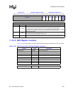


SA-1110 Developer’s Manual 389
Peripheral Control Module
give control of the pins back to the peripheral units. Note that sleep mode invocation causes RPP to be
cleared so that the pins are once again held in their sleep state until the user can set RPP. See
Chapter 9, “System Control Module”.
Because the peripherals are reset when sleep mode is entered, serial port 2’s transmit and receive
pin (TXD2 and RXD2) polarity bits (TXP and RXP) are both reset to one, which configures
transmit and receive data as true or noninverted data. Thus the user need not reprogram these bits
prior to the invocation of sleep mode.
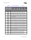
Note that PSDR is initialized only by a hardware or power-on reset (negation of the nRESET pin). It
is not affected by a software reset or a reset that occurs as a result of the SA-1110 entering sleep
mode. Also note that for reserved bits, writes are ignored and reads return zero. The following table
shows the location of each sleep mode pin direction bit and to which peripheral pin it corresponds.
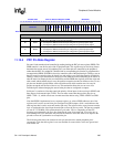
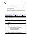
0h 9006 000C
PPC Pin Sleep Mode Direction
Register: PSDR
Read/Write
31 30 29 28 27 26 25 24 23 22 21 20 19 18 17 16 15 14 13 12 11 10 9 8 7 6 5 4 3 2 1 0
Reserved
SFRM
SCLK
RXD4
TXD4
RXD3
TXD3
RXD2
TXD2
RXD1
TXD1
L_BIAS
L_FCLD
L_LCLK
L_PCLK
LDD 7
LDD 6
LDD 5
LDD 4
LDD 3
LDD 2
LDD 1
LDD 0
0 0 0 0 0 0 0 0 0 0 1 1 1 1 1 1 1 1 1 1 1 1 1 1 1 1 1 1 1 1 1 1
(Sheet 1 of 2)
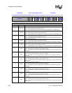
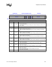
Bits Name Description
7..0 LDD 7..0
LCD data sleep mode pin direction.
0 – LCD data pin configured as output and is driven low during sleep.
1 – LCD data pin configured as input during sleep.
8 L_PCLK
LCD pixel clock sleep mode pin direction.
0 – LCD pixel clock pin configured as output and is driven low during sleep.
1 – LCD pixel clock pin configured as input during sleep.
9 L_LCLK
LCD line clock sleep mode pin direction.
0 – LCD line clock pin configured as output and is driven low during sleep.
1 – LCD line clock pin configured as input during sleep.
10 L_FCLK
LCD frame clock sleep mode pin direction.
0 – LCD frame clock pin configured as output and is driven low during sleep.
1 – LCD frame clock pin configured as input during sleep.
11 L_BIAS
LCD ac bias sleep mode pin direction.
0 – LCD ac bias pin configured as output and is driven low during sleep.
1 – LCD ac bias pin configured as input during sleep.
12 TXD1
Serial port 1: UART transmit sleep mode pin direction.
0 – Transmit pin configured as output and is driven low during sleep.
1 – Transmit pin configured as input during sleep.
13 RXD1
Serial port 1: UART receive sleep mode pin direction.
0 – Receive pin configured as output and is driven low during sleep.
1 – Receive pin configured as input during sleep.
14 TXD2
Serial port 2: IPC transmit sleep mode pin direction.
0 – Transmit pin configured as output and is driven low during sleep.
1 – Transmit pin configured as input during sleep.
15 RXD2
Serial port 2: IPC receive sleep mode pin direction.
0 – Receive pin configured as output and is driven low during sleep.
1 – Receive pin configured as input during sleep.