


124 SA-1110 Developer’s Manual
Memory and PC-Card Control Module
10.1.6 Aborts and Nonexistent Memory
Reads from reserved address locations (as specified in the memory map) will result in a data abort
exception. Writes to reserved address space will have no effect.
Reads and writes from or to nonexistent memory are not detected in hardware. In case no memory
is selected on a read, the value last driven on the data bus is returned.
A single access to a disabled DRAM bank (MDCNFG:DEx=0) will cause a CBR refresh cycle to
all banks. This technique is used in the hardware and sleep reset procedures (see Section 10.2.1)
and the software and watchdog reset procedures (see Section 10.2.2). Zeros are returned to the
register file on reads, writes are dropped. A burst read access to a disabled DRAM bank will result
in a data abort exception.
10.2 Memory Interface Reset and Initialization
Note: This section contains numerous references to the memory configuration registers. The memory
configuration registers are discussed in Section 10.3.
On hardware or sleep reset, the dynamic memory interface is disabled. The boot ROM (connected
to nCS0) is configured for SMROM if SMROM_EN=1. Otherwise, boot ROM is configured for
the slowest nonburst ROM/Flash. The ROM_SEL pin determines the bus size of asynchronous
boot ROM (ground = 16 bit, high = 32 bit). Immediately, boot ROM is available for reading and all
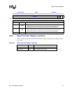
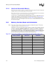
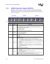
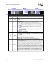
memory interface control registers are available for reading and writing. Table 10-6 summarizes
the state of the memory pins and memory controller after a hardware reset.
Figure 10-2. Memory Pins and Memory Controller State after Hardware Reset (Sheet 1 of 2)
SIGNAL or REGISTER RESET VALUE DESCRIPTION
nRAS/nSDCS[3:0] 0xF DRAM RAS or SDRAM CS
nCAS/DQM[3:0] 0xF DRAM CAS or SDRAM DQM
nCS[5:0] 0x3F Static chip selects
nOE 1 Memory output enable
nWE 1 Memory write enable
RD/nWR 0 Read/write direction control
nPIOR 1 PCMCIA I/O read
nPIOW 1 PCMCIA I/O write
nPOE 1 PCMCIA output enable
nPWE 1 PCMCIA write enable
nSDRAS 1 SDRAM RAS
nSDCAS 1 SDRAM CAS
SDCKE 0 SMROM_EN SDRAM or SMROM clock enable
SDCKE 1 0 SDRAM or SMROM clock enable