


302 SA-1110 Developer’s Manual
Peripheral Control Module
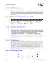
11.10.1.2 UART Frame Format
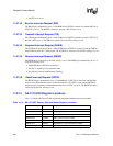
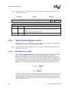
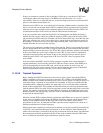
For transmission rates up to 115.2 Kbps, the ICP’s UART is used. The user must program it to
produce a frame that produces 8 bits of data, one stop bit, and no parity, as shown in Figure 11-23.
Note that PE=1, SBS=1, DSS=0, SCE=1, BRK=1, RXE=0, TXE=0, and BRD=0x000 are illegal
programming modes for IrDA operation and will produce unpredictable results. See Section 11.11,
“Serial Port 3 – UART” on page 11-325 for a complete description of how to program and operate
the ICP’s UART.
Figure 11-23. UART Frame Format for IrDA Transmission (<= 115.2 Kbps)
11.10.2 High-Speed ICP Operation
Before enabling the ICP for high-speed operation, the user must first clear any writable or “sticky”
status bits that are set by writing a one to each bit. Next, the desired mode of operation is
programmed in the control registers. At this point the user can “prime” the HSSP’s transmit FIFO
by writing up to 16 values, or the FIFO can remain empty and either programmed I/O or the DMA
can be used to service it after the HSSP is enabled. Once the HSSP is enabled,
transmission/reception of data can begin on the transmit (TXD2) and receive (RXD2) pins.
For high-speed operation, all serial data, which is transferred between the TXD2/RXD2 pins and
the ICP’s HSSP, is modulated/demodulated according to the 4PPM IrDA standard. For high-speed
transmission, both the modulation technique and the HSSP’s frame format are discussed in the
following sections.
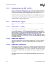
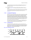
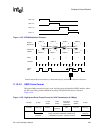
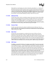
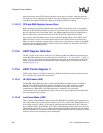
11.10.2.1 4PPM Modulation
Four-position pulse modulation (4PPM) is used for the high-speed transmission rate of 4.0 Mbps.
Two data bits are encoded at a time by placing a single 125 ns light pulse within one of four time
slots. The four time slots are collectively termed a “chip.” Bytes are encoded one at a time. They
are divided into four individual nibbles (2-bit pairings) and the least significant nibble is
transmitted first. Figure 11-24 shows the 4PPM encoding for the four possible 2-bit combinations
and Figure 11-25 shows an example of 4PPM modulation of the byte 8’b10110001 that is
constructed using four chips. Note that bits within each nibble are not reordered, but nibble 0 (least
significant) is transmitted first, ending with nibble 3 (most significant).
Figure 11-24. 4PPM Modulation Encodings
Start Bit Data 7 Data 6 Data 5 Data 4 Data 3 Data 2 Data 1 Data 0 Stop Bit
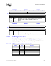
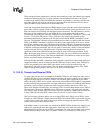
UTCR0-2 Programming:
PE=0 DSS = 1 TCE = don’tcare RXE=1 RIE=0or1
OES = don’tcare SCE=0
BRD = 0x001 to
0xFFF
TXE = 1 TIE = 0 or 1
SBS = 0 RCE = don’tcare BRK=0
Chip
Timeslots
1234