


SA-1110 Developer’s Manual 171
Memory and PC-Card Control Module
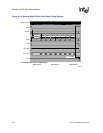
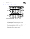
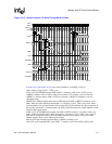
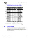
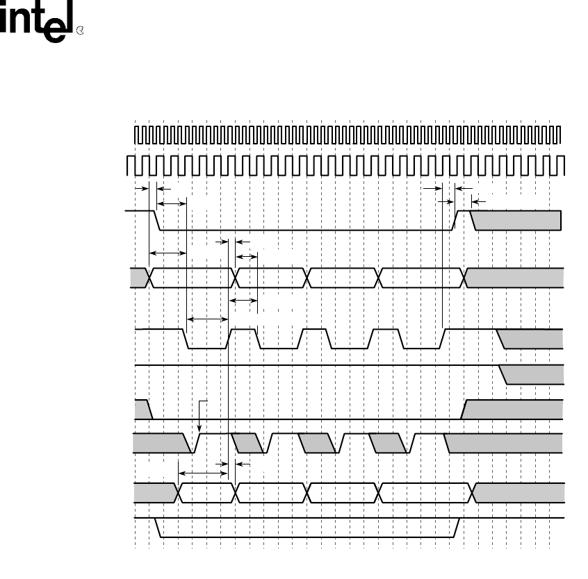
Figure 10-15. Variable Latency I/O Write Timing (Burst-of-Four)
In Figure 10-14 and Figure 10-15, some of the parameters are defined as follows:
tAS = Address setup to nCS = 1 CPU cycle
tCES = nCS, nCAS/DQM setup to nOE or nWE = 2 memory clock cycles (4 CPU cycles)
tASRW0 = Address setup to nOE or nWE low (asserted) = 2.5 memory cycles on first beat
tASRWN = Address setup to nOE or nWE low (asserted) = (RDN+0.5) memory cycles on
subsequent beats
tDSWH,min = Minimum Write data setup to nWE high (deasserted) = (RDF+1.5) memory cycles
tDH = Data hold after nWE high (deasserted) = 1/2 memory cycle (1 CPU cycle). Note: After a
write transaction, the last data remains driven on the D[31:0] pins until the next bus transaction. If
the next bus transaction is a read operation, the D[31:0] pins are released to a high impedance state
when the nOE signal asserts.
tCEH = nCS, nCAS/DQM held asserted after nOE or nWE deasserted = 1 memory clock cycle
tAH = Address hold after nOE or nWE deasserted = 1/2 memory cycle (1 CPU cycle). Note: If
there are no subsequent memory bus transactions after the access (read or write), the current
address remains driven on the address pins A[25:0].
nOE or nWE high time between burst beats = (RDN+1) memory cycle.
tSS = CPU starts sampling RDY signal (RDF - 1) memory cycles after nOE or nWE asserts.
A6655-02
CPU
Clock
Memory
Clock
A(25:0)
nCS4
nOE
RD/nWR
D(31:0)
RDY
nWE
D3D1D0 D2
t
AS
t
CES
t
ASRW0
RDF+1+WAITS
RDN+1
t
DSWH
t
CEH
max(2
*
RRR,1)
t
AH
t
ASRWN
A0 A0+4 A0+8 A0+12
nCAS[3:0]
t
DH
t
SS
Note: RDF = 2, RDN = 1, WAITS = 0 for this figure