


136 SA-1110 Developer’s Manual
Memory and PC-Card Control Module
10.3.3 CAS Waveform Rotate Registers (MDCAS00, MDCAS01,
MDCAS02, MDCAS20, MDCAS21, MDCAS22)
MDCAS00, MDCAS01, and MDCAS02 are 32-bit read/write registers that contain the nCAS
waveform for a burst read or write to asynchronous DRAM within DRAM bank pair 0/1. They also
control the RAS-to-CAS delay and read data latching edges for SDRAM within DRAM bank
pair 0/1 and SMROM within static bank pair 0/1 (nCS 0 and nCS 1).
For asynchronous DRAM, each bit represents one CPU cycle if MDCNFG:CDB20 is "0", 2 CPU
cycles (one memory clock cycle) if MDCNFG:CDB20 is "1" or MDCNFG:DWID0 is "1". DWID0
overrides CDB20 because the DRAM state machine supports 16-bit data-busses only if each half of
a full-word access occurs on the memory clock’s rising edge. For SDRAM and SMROM, each bit
always represents one CPU cycle. Question marks indicate that the values are unknown at hardware
or sleep reset.
MDCAS20, MDCAS21, and MDCAS22 are 32-bit read/write registers that provide the same
functionality for asynchronous DRAM or SDRAM within DRAM bank pair 2/3 and SMROM
within static bank pair 2/3 (nCS 2 and nCS 3), as a function of MDCNFG:CDB22 and
MDCNFG:DWID2.
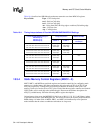
The hardware or sleep reset value for MDCAS00 (shown below) supports SMROM single word
reads at one-half the memory clock frequency (MDREFR:K0DB2=1), with a RAS-to-CAS delay
of two cycles. If SMROM_EN=1, this value must be maintained to avoid a mismatch in RAS
latency between the SA-1110 and boot SMROM following a subsequent hardware or sleep reset.
10.3.3.1 MDCAS Registers with Asynchronous DRAM
When asynchronous DRAM is accessed, the least significant bit of MDCAS00 goes out first and is
the cycle coincident with the assertion of nRAS/nSDCS. Bit 1 is one cycle after the assertion of
nRAS/nSDCS, and so forth. MDCAS01 is appended after MDCAS00 and MDCAS02 is appended
after MDCAS01. A "1" in any field causes nCAS/DQM to be deasserted in that cycle and a "0"
causes nCAS/DQM to be asserted in that cycle. The memory controller counts nCAS/DQM pulses
and deasserts nRAS/nSDCS in the cycle following the deassertion of the final nCAS/DQM pulse of
the burst. For optimum performance, all nCAS/DQM pulses should be programmed. However, if
there are not enough programmed pulses to complete all of the beats in a transfer after the most
significant bit of MDCAS002 is reached, the rotate registers will start over from the least significant
bit of MDCAS00 and continue to rotate until the transfer is complete.
When MDCNFG:CDB20 is "0"and MDCNFG:DWID0 is "0", the MDCAS00 must contain "1"s in
the lower 4 bits and each transition of nCAS/DQM must be a minimum of 2 clocks (so
nCAS/DQM must be asserted for a minimum of 2 CPU clock cycles and deasserted for a minimum
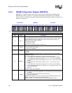
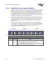
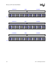
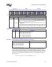
0h A000 0004 MDCAS00 Read/Write
31 30 29 28 27 26 25 24 23 22 21 20 19 18 17 16 15 14 13 12 11 10 9 8 7 6 5 4 3 2 1 0
C00_31
C00_30
C00_29
C00_28
C00_27
C00_26
C00_25
C00_24
C00_23
C00_22
C00_21
C00_20
C00_19
C00_18
C00_17
C00_16
C00_15
C00_14
C00_13
C00_12
C00_11
C00_10
C00_9
C00_8
C00_7
C00_6
C00_5
C00_4
C00_3
C00_2
C00_1
C00_0
Reset ? ? ? ? ? ? ? ? ? ? ? ? ? ? ? ? ? ? ? ? 0 1 0 1 0 1 1 1 1 1 1 1