


374 SA-1110 Developer’s Manual
Peripheral Control Module
11.12.10 SSP Control Register 1
The SSP control register 1 (SSCR1) contains six different bit fields that control various functions
within the SSP.
11.12.10.1 Receive FIFO Interrupt Enable (RIE)
The receive FIFO interrupt enable (RIE) bit is used to mask or enable the receive FIFO service
request interrupt. When RIE=0, the interrupt is masked and the state of the receive FIFO service
request (RFS) bit within the SSP status register is ignored by the interrupt controller. When RIE=1,
the interrupt is enabled, and whenever RFS is set (one), an interrupt request is made to the interrupt
controller. Note that programming RIE=0 does not affect the current state of RFS or the receive
FIFO logic’s ability to set and clear RFS, it only blocks the generation of the interrupt request. Also
note that RIE does not affect generation of the receive FIFO DMA request, which is asserted
whenever RFS=1.
11.12.10.2 Transmit FIFO Interrupt Enable (TIE)
The transmit FIFO interrupt enable (TIE) bit is used to mask or enable the transmit FIFO service
request interrupt. When TIE=0, the interrupt is masked and the state of the transmit FIFO service
request (TFS) bit within the SSP status register is ignored by the interrupt controller. When TIE=1,
the interrupt is enabled, and whenever TFS is set (one), an interrupt request is made to the interrupt
controller. Note that programming TIE=0 does not affect the current state of TFS or the transmit
FIFO logic’s ability to set and clear TFS; it only blocks the generation of the interrupt request. Also
note that TIE does not affect generation of the transmit FIFO DMA request, which is asserted
whenever TFS=1.
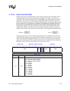
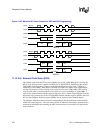
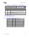
5..4 FRF
Frame Format.
00 – Motorola SPI frame format.
01 – Texas Instruments Synchronous serial frame format.
10 – National Microwire frame format.
11 – Reserved, undefined operation.
6 — Reserved.
7SSE
Synchronous serial port enable.
0 – SSP operation disabled, control of pins given to PPC if MCP is also disabled.
1 – SSP operation enabled if MCP disabled or if the PPC SSP pin reassignment bit is set
(reassigns GPIO 13..10 to the SSP).
15..8 SCR
Serial clock rate.
Value (from 0 to 255) used to generate the transmission rate of the SSP.
Bit Rate = 3.6864x10
6
/(2x(SCR+1)), where SCR is a decimal value.
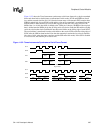
0h 8007 0060 SSP Control Register 0: SSCR0 Read/Write
15 14 13 12 11 10 9 8 7 6 5 4 3 2 1 0
SCR SSE
Reserved
FRF DSS
? ? ? ? ? ? ? ? 0 0 ? ? ? ? ? ?
(Sheet 2 of 2)
Bits Name Description