


SA-1110 Developer’s Manual 403
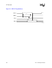
AC Parameters
NOTES:
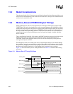
1. The LCD data pins can be programmed to be driven on either the rising or falling edge of the pixel clock
(L_PCLK).
2. These LCD signals can, at times, transition when L_PCLK is not clocking (between frames). At this time, they
are clocked with the internal version of the pixel clock before it is driven out onto the L_PCLK pin.
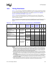
13.6.1 Asynchronous Signal Timing Descriptions
The list below describes lists and describes asynchronous timing signals.
• nPWAIT is an input and is received through a synchronizer. As such, it has no setup and hold
specification. The user must adhere to the protocol definition.
• When the peripheral pins are in GPIO mode, they are read or written under software control.
As outputs, they are driven valid on the pin approximately 20 ns after they are written by
software. When inputs, they are received by a synchronizer and must be valid for
approximately 20 ns before they are able to be recognized by a CPU read.
• nRESET must remain asserted for 150 ms after VDD and VDDX are stable to properly reset
the SA-1110.
• nRESET_OUT is asserted for all types of reset (hard, watchdog, sleep, and software) and
appears on the pin asynchronously to all clocks.
• BATT_FAULT and VDD_FAULT are asynchronous inputs and are synchronized to the
32.768-kHz clock after entering the SA-1110. They must be valid for approximately 60 ms
before they are recognized by the SA-1110.
• PWR_EN asserts when the SA-1110 enters sleep mode and is driven onto the pin following the
rising edge of the 32.768-kHz clock. It negates on the same edge as sleep mode is exited.
• GP[27:0] are read and written under software control. In addition, an asynchronous edge
detect may be performed. When writing a value to these pins, the pin transitions approximately
20 ns after the write is performed. When reading these pins, the signal is first synchronized to
the internal memory clock and must be valid for at least 20 ns before it is visible to a processor
read. For edge detects, the value on the pin following an edge must be stable for at least 10 ns
for the edge to be caught by the edge detect circuit.
• UDC+, UDC-, TXD_1, RXD_1, TXD_2, RXD_2, TXD_3, and RXD_3 are asynchronous
relative to any device outside the SA-1110. The output pins, like all outputs on the SA-1110,
have been characterized while driving a 50-pF lumped load capacitance.
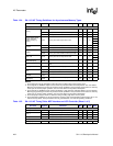
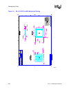
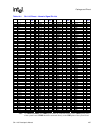
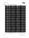
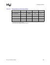
L_LCLK Tpclklv L_PCLK fall/rise to L_LCLK driven valid — 14 ns 2
L_FCLK Tpclkfv L_PCLK fall/rise to L_LFCLK driven valid — 14 ns 2
L_BIAS
Tpclkbv
L_PCLK rise/fall to L_BIAS driven valid
— 14 ns 2
Table 13-5. SA-1110 AC Timing Table: MCP Interface and LCD Controller (Sheet 2 of 2)
Pin Name Symbol Parameter Min Max Unit Note