


SA-1110 Developer’s Manual 213
Peripheral Control Module
be from the device to memory. The transfer direction is fixed for each device type. If the device
data transfer direction is programmed incorrectly for a particular device select, then the results are
unpredictable.
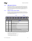
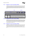
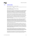
11.6.1.2 DMA Control/Status Register (DCSRn)
DCSR1 - DCSR5 are each a group of three 32-bit read/write registers which contain control and
status bits for the channel (refer to Section 11.6.2, “DMA Register List” on page 11-217 for
physical addresses and functions of each group). The following figure shows the format for this
register; question marks indicate the values are unknown at reset.
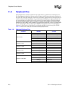
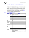
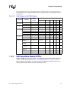
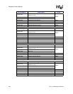
Table 11-6. Valid Settings for the DDARn Register
Unit Name Function
Device
Address
DDAR Fields
DA[31:8] DS[3:0] DW BS E RW
Serial port 0
UDC transmit 0x 8000 0028
0x80000A 0000 0 1 0/1 0
UDC receive 0x 8000 0028 0x80000A 0001 0 1 0/1 1
Serial port 1 UART transmit 0x 8001 0014
0x804005 0100 0 0 0/1 0
UART receive 0x 8001 0014 0x804005 0101 0 0 0/1 1
Serial port 2 HSSP transmit 0x 8004 006C
0x81001B 0110 0 1 0/1 0
HSSP receive 0x 8004 006C
0x81001B 0111 0 1 0/1 1
UART transmit 0x 8003 0014 0x80C005 0110 0 0 0/1 0
UART receive 0x 8003 0014 0x80C005 0111 0 0 0/1 1
Serial port 3 UART transmit 0x 8005 0014
0x814005 1000 0 0 0/1 0
UART receive 0x 8005 0014 0x814005 1001 0 0 0/1 1
Serial port 4 MCP transmit
(audio)
0x 8006 0008
0x818002 1010 1 0 0/1 0
MCP receive
(audio)
0x 8006 0008 0x818002 1011 1 0 0/1 1
MCP transmit
(telecom)
0x 8006 000C
0x818003 1100 1 0 0/1 0
MCP receive
(telecom)
0x 8006 000C 0x818003 1101 1 0 0/1 1
SSP transmit 0x 8007 006C
0x81C01B 1110 1 0 0/1 0
SSP receive 0x 8007 006C 0x81C01B 1111 1 0 0/1 1