


SA-1110 Developer’s Manual 125
Memory and PC-Card Control Module
On sleep reset, the memory pins and controller are in the same state as after hardware reset; except
that the nCAS/DQM and nRAS/nSDCS pins remain asserted (nCAS/DQM[3:0] = 0 and
nRAS/nSDCS[3:0] = 0) to keep asynchronous DRAM in self-refresh until the processor can be
configured. nRAS/nSDCS and nCS 0 are asserted simultaneously because that latter is needed to
fetch instructions from the reset vector. If SDRAM were in self-refresh, they are kept there by
having SDCKE(1) = 0.
10.2.1 Hardware or Sleep Reset Procedures
Software is responsible for controlling the following procedures when coming out of hardware or
sleep reset. The procedures are slightly different for hardware reset and sleep reset.
1. On hardware reset in systems with DRAM or SDRAM, complete a power-on wait period
(typically 100-200µsec). This allows the internal clocks (used to generate SDCLK) to
stabilize.
2. In systems containing SMROM, write to SMCNFG to configure the CAS latencies
(CL fields), row address bit counts (RA fields), and enables (SM bits). A careful software
sequence, involving a subsequent write to SMCNFG, is required to change RAS latencies
(RL fields): see Section 10.4.1. While any SMROM banks are being configured, all SDRAM
banks and SDRAM/SMROM auto-power-down must be disabled.
3. On sleep reset in systems containing DRAM, see Section 9.5 on how to release the
nCAS/DQM and nRAS/nSDCS pins so that the DRAM will exit self-refresh.
4. In systems containing SDRAM, transition the SDRAM controller through the following state
sequence: "self-refresh and clock-stop" to "self-refresh" to "power-down" to "PWRDNX" to
"idle". See Figure 10-5. The SDRAM clock run and enable bits (K1RUN, K2RUN, and
E1PIN) are described in Section 10.3.2.
5. Appropriately configure, but do not enable, each DRAM bank pair for asynchronous DRAM
or SDRAM.
6. On hardware reset in systems containing DRAM or SDRAM, trigger a number (typically
eight) of refresh cycles by attempting nonburst read or write accesses to any disabled DRAM
bank. Each such access causes a simultaneous CBR for all four banks: each bank pair
according to its DRAM or SDRAM configuration. For SDRAM, it does this by causing a pass
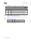
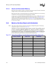
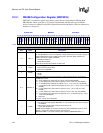
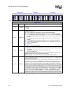
SDCLK 0
if the pin SMROM_EN=1,
SDCLK 0 oscillates at 1/2 the
memory clock frequency (1/4 the
CPU frequency)
if the pin SMROM_EN=0,
SDCLK 0 does not
oscillate
SDCLK 0 frequency
SDCLK 1 and SDCLK 2 0 SDCLK 1 and SDCLK 2 disabled
Register MDCNFG:DE3-0 0 All DRAM banks disabled
Register MSC0:[15:0]
set to SMROM or slowest
non-burst ROM/FLASH timing.
(MSC0:[15:0] field is initialized as
follows: RRR=0xF, RDN=0x1F,
RDF=0x1F, RBW = not
ROM_SEL, RT=0)
Static interface configuration
Figure 10-2. Memory Pins and Memory Controller State after Hardware Reset (Sheet 2 of 2)
SIGNAL or REGISTER RESET VALUE DESCRIPTION