


326 SA-1110 Developer’s Manual
Peripheral Control Module
11.11.1.1 Frame Format
Each data frame is between 9 bits and 12 bits long depending on the size of data programmed, if
parity is enabled and if a second stop bit is enabled. The frame begins with a start bit that is
represented by a high to low transition. Next, either 7 bits or 8 bits of data are transmitted,
beginning with the least significant bit. An optional parity bit follows, which is set if even parity is
enabled and an odd number of ones exist within the data byte, or if odd parity is enabled and the
data byte contains an even number of ones. The data frame ends with either one or two stop bits as
programmed by the user, which is represented by one or two successive bit periods of a logic one.
Note that the receiver only tests for one stop bit per frame.
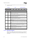
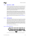
11.11.1.2 Baud Rate Generation
The baud or bit rate is derived by dividing down the 3.6864-MHz clock generated by the on-chip
PLL. The clock is first divided by a programmable number between 1 and 4096, and then by a
fixed value of 16. The receive baud clock is synchronized with the data stream using a digital PLL
each time the start bit is detected on the receive data line. Receive data is then sampled halfway
through each bit period by counting 8 of the 16 clocks, which are produced before the fixed divide
by 16 takes place. (See Figure 11-27.)
11.11.1.3 Receive Operation
The UART receives incoming data by using a serial shifter. It latches the frame, strips it of its start,
parity, and stop bits, and then places the data within receive FIFO. If parity is enabled, the number
of data bits, which is one, is counted as data and is extracted from each frame. Parity is then
checked by comparing this value to the stripped parity bit. Either odd or even parity is checked as
specified by the programmer. If a parity error is detected, the parity error bit is set in the FIFO entry
corresponding to the data value that caused the error. Additionally, if a logic zero is detected by the
receive logic where a stop bit was expected, the framing error bit is set in the FIFO entry
corresponding to the errant data. When the FIFO fills between one- to two-thirds full, an interrupt
or DMA request is signalled. If the FIFO is completely filled and the receive logic attempts to place
additional data within the FIFO, the overrun bit is set next to the last byte of data received within
the FIFO. Any data received while the FIFO is completely full is discarded.
The parity, framing, and overrun error bits are transferred down the receive FIFO along with the data
that caused the error. Whenever any of the four bottom FIFO entries contain one or more error bits that
are set, an interrupt is generated and receive FIFO DMA requests are disabled until the error is flushed
from the FIFO and the status bit that signalled the interrupt is cleared. At this point, the user should use
programmed I/O to check the error bits and remove data one piece at a time until the four FIFO entries
are flushed. Each time a data value is transferred to the bottom of the FIFO, the state of the parity,
framing, and overrun bits within the last FIFO entry are automatically transferred to their respective
flag bits in the status register. When any of these three flags are set in the UART status register, it
indicates that the next data value available within the FIFO contains an error. The user must first check
the state of these three flags to see if the next value within the FIFO contains an error, then read the
FIFO value. After four values have been removed from the FIFO and the errors are identified, the
DMA is automatically reenabled once the error in FIFO bits are removed from the FIFO.
If the receive FIFO contains valid data and three frame periods elapse without the reception of data
on RXD3, the receiver idle interrupt is generated. Also, if the receive logic detects a null character
(all zeros, including the parity bit) followed by a framing error (stop bit is zero as well), the receive
logic generates a beginning of break detect, which interrupts the CPU. Because breaks can be
signalled for long periods of time, after the break is negated and the receive pin transitions high, the
receive logic generates an end of break detect, which again interrupts the CPU.