


SA-1110 Developer’s Manual 35
Functional Description
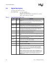
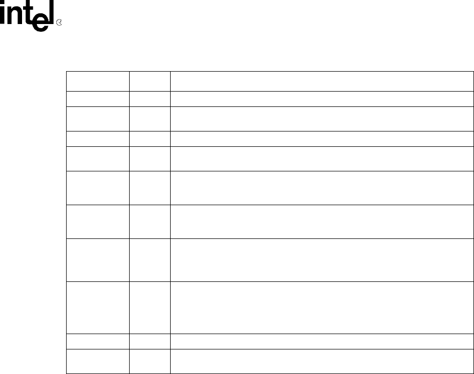
TDI IC JTAG test interface data input. Note this pin has an internal pull-up resistor.
TDO OCZ JTAG test interface data output. Note this pin does not have an internal pull-up
resistor.
TMS IC JTAG test interface mode select. Note this pin has an internal pull-up resistor.
TCK IC JTAG test interface reference clock. This times all the transfers on the JTAG test
interface. Note this pin has an internal pull-down resistor.
TCK_BYP IC Test clock PLL bypass. When TCK_BYP is high, the TESTCLK is used as the
core clock in place of the PLL clock; when low, the internal PLL output is used.
This signal has no relation to the JTAG TCK pin.
TESTCLK IC Test clock. TESTCLK is used to provide the core clock when TCK_BYP is high. It
should be tied low if TCK_BYP is low. This pin should be used for test purposes
only. An end user should ground this pin.
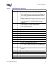
VDD — Positive supply for the core. Nine pins are allocated to this supply; eight pins are
labeled VDD. The ninth pin, labeled VDDP is dedicated to the PLL supply and
should have its own dedicated decoupling capacitor. Also, it should be tied directly
to the VDD power plane with the other eight VDD pins.
VDDX — Positive supply for the pins. See Chapter 14 for a count of VDDX pins. All of the
pins allocated to VDDX (labeled VDDX1, VDDX2, and VDDX3) should be tied
directly to the VDDX power plane and are all required to remain powered up at all
times for proper device operation. VDDX3 is connected to an internal voltage
regulator and should have its own dedicated decoupling capacitor.
VSS — Ground supply. Nine pins are allocated to VSS, including one for the PLL.
VSSX — Ground supply for the I/O pins. See Chapter 14, “Package and Pinout,” for a count
of VSSX pins.
Table 2-1. Signal Descriptions (Sheet 4 of 4)
Name Type Description