


SA-1110 Developer’s Manual 167
Memory and PC-Card Control Module
10.6.3 SRAM Interface Overview
The SA-1110 provides a 16-bit or 32-bit asynchronous SRAM interface that uses the nCAS/DQM
pins for byte selects on both reads and writes. nCS[2:0] select the SRAM bank, nOE is asserted on
reads and nWE is asserted on writes. Address bits A[25:2] provide addressability of up to
64Mbytes of SRAM per bank.
The SA-1110 supports systems with both SRAM and DRAM (synchronous or asynchronous) by
ensuring at least one-and-a-half memory clocks of nCAS/DQM[3:0] deassertion between any
permutation of SRAM (or variable latency I/O) access and DRAM activity (access, CBR, or
self-refresh). However, the recovery time between SRAM accesses (RRR[2:0]) must be set to
satisfy the minimum nCAS/DQM[3:0] deassertion time for any asynchronous DRAM present in
the system.
The timing for a read access is identical to that for a nonburst ROM (see Section 10.6.2). The RDF
fields in the MSCx registers are the latency for a read access. The MSCx:RDN field controls the
nWE low time during a write cycle. MSCx:RRR is either the time from nCS deassertion after a
read to the start of an access from a different memory bank, or the time from nCS deassertion after
a write to the start of any other memory access (read or write, same or different bank). The
MSCx:RRR delay is not applied between subsequent reads from the same bank. MSCx:RT must
select SRAM.
A single CBR refresh cycle, for asynchronous DRAM and/or SDRAM, may be inserted between
word accesses within a burst transaction. nCS, nOE, and nWE are deasserted during the refresh
cycle.
Note: Using SRAM with nCS[2:0] results in higher memory read access performance than using SRAM
with nCS[5:3] and RDY tied high. See Section 10.6.5 and refer to Figure 10-12 and Figure 10-14
timing diagrams to calculate performance difference.
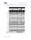
10.6.4 SRAM Timing Diagrams and Parameters
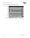
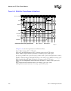
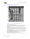
As shown in Figure 10-11, SRAM reads have the same timing as nonburst ROMs, except
nCAS/DQM[3:0] are used as byte selects and are asserted with the same timing as nCS. When
nCAS/DQM0 is low (asserted), D[7:0] will be used to transfer data. When nCAS/DQM1 is low,
D[15:8]isused,andsoforth.Duringwrites,all32datapinsareactivelydrivenbytheSA-1110
(that is, they are not tristated) regardless of the state of the individual nCAS/DQM pins.
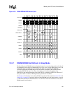
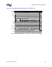
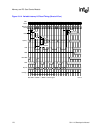
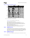
Figure 10-13 shows the timing for SRAM writes.