


SA-1110 Developer’s Manual 305
Peripheral Control Module
11.10.2.7 Baud Rate Generation
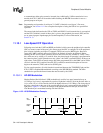
The baud rate is derived by dividing down a fixed 48-MHz clock generated by one of the two
on-chip PLLs by six. The 8-MHz baud clock (or time slot) for the receive logic is synchronized
with the 4PPM data stream each time a transition is detected on the receive data line using a digital
PLL. To encode a 4-Mbps data stream, the required “chip” frequency is 2.0 MHz, with four time
slots per chip at a frequency of 8.0 MHz. Receive data is sampled halfway through each time-slot
period by counting three out of the six 48-MHz clock periods that make up each time slot (see
Figure 11-25). The chips are synchronized during preamble reception. The repeating pattern (four
chips repeated 16 times) is used to identify the first time slot or beginning of a chip and resets the
2-bit time-slot counter logic, such that the 4PPM data is properly decoded.
11.10.2.8 Receive Operation
The IrDA standard specifies that all transmission occurs at half-duplex. This restriction forces the
user to enable one direction at a given time: either the transmit or receive logic, but not both.
However, the HSSP’s hardware does not impose such a restriction.The user may enable both the
transmitter and receiver at the same time. Although forbidden by the IrDA standard, this feature is
particularly useful when using the ICP’s loopback mode, which internally connects the output of
the transmit serial shifter to the input of the receive serial shifter.
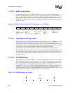
After the ICP is enabled for 4-Mbps transmission, the receiver logic begins by selecting an
arbitrary chip boundary, receives four incoming 4PPM chips from the RXD2 pin using a serial
shifter, and latches and decodes the chips one at a time. If the chips do not decode to the correct
preamble, the time-slot counter’s clock is forced to skip one 8-MHz period, effectively delaying the
time-slot count by one. This process is repeated until the preamble is recognized, signifying that
the time-slot counter is synchronized. The preamble can be repeated as few as 16 times or may be
continuously repeated to indicate an idle receive line.
At any time after the transmission of 16 preambles, the start flag can be received. The start flag is
eight chips long. If any portion of the start flag does not match the standard encoding, the receive
logic signals a framing error and the receive logic once again begins to look for the frame
preamble.
Once the correct start flag is recognized, each subsequent grouping of four chips is decoded into a
data byte and placed within a 5-byte temporary FIFO, which is used to prevent the CRC from being
placed within the receive FIFO. When the temporary FIFO is filled, data values are pushed out one
by one to the receive FIFO. The first data byte of a frame is the address. If receiver address
matching is enabled, the received address is compared to the address programmed in the address
match value field in one of the control registers. If the two values are equal or if the incoming
address contains all ones, all subsequent data bytes, including the address byte, are stored in the
receive FIFO. If the values do not match, the receiver logic does not store any data in the receive
FIFO, ignores the remainder of the frame, and begins to search for the next preamble. The second
data byte of the frame can contain an optional control field as defined by the user and must be
decoded in software (no hardware support within the HSSP).
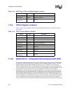
CRC x() x
32
x
26
x
23
x
22
x
16
x
12
x
11
x
10
x
8
x
7
x
5
x
4
x
2
x 1+ + + + + + + +++++++( )=