


122 SA-1110 Developer’s Manual
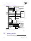
Memory and PC-Card Control Module
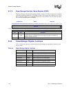
The PC-Card interface provides control signals to support a single PC-Card card slot with
additional hooks to support two slots. It shares address and data pins with the memory devices. It
uses address lines, A[25:0], and data lines, D[15:0]. nPREG is actually A 26 and selects register
space (I/O or attribute) versus memory space. nPOE and nPWE are provided for memory and
attribute reads and writes. nPIOR, nPIOW, and nIOIS16 input control I/O reads and writes.
nPWAIT allows for extended access times. nPCE2 and nPCE1 are byte select high and low,
respectively. PSKTSEL selects between two card slots.
This interface also supports 32-bit accesses that are outside the PC-Card specification. See
Section 10.7 for information about restrictions for the use of this feature.
• Alternate Memory Bus Master Mode
The SA-1110 supports an alternate master on the DRAM memory bus in which an external master
is given control of the bus using a hardware handshake. This handshake is performed using the
alternate GPIO functions, MBREQ and MBGNT. The alternate master initiates taking control of
the memory bus by asserting MBREQ. The SA-1110 completes any pending or in-progress
memory operations and any outstanding DRAM refresh cycle. The SA-1110 then deasserts
SDCKE 1 and three-states all memory bus pins used with DRAM bank 0. All other memory and
PCMCIA pins remain driven. The SA-1110 then responds to the external master by asserting
MBGNT indicating to the alternate master that it should start driving all pins (including SDCLK
1). The SA-1110 will re-assert SDCKE 1. The alternate master must assume the responsibility for
DRAM integrity while in this mode since the SA-1110 is unable to perform DRAM refresh cycles
during the three-state period. When the alternate bus master is ready to release the bus, the external
master deasserts MBREQ; the SA-1110 acknowledges by deasserting SDCKE 1 and MBGNT. The
alternate master stops driving the DRAM pins (including SDCLK 1), and the SA-1110 resumes
driving all DRAM pins (including SDCLK 1) and re-asserts SDCKE 1.
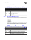
10.1.1 Types of Memory Accesses
The SA-1110 performs memory accesses for the following operations:
SA-1110 will only generate a subset of all possible transactions on the bus. Many of these
transactions may be completed internal to the processor by accessing caches, the read buffer,
on-chip registers, or the special memory space (128 Mbytes starting at physical address
0xE000 0000) that returns zeroes for flushing the cache.
If a memory access is followed by an idle period on the bus, the control signals return to their
inactive state and the address and data signals remain at their previous values to avoid unnecessary
bus transitions and eliminate the need for pull-up resistors.
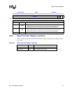
10.1.2 Reads
Read bursts are generated by DMA requests, read buffer requests, and cache line fills. All line fills
(for instruction and data caches) are eight words long. DMA and read buffer requests are one, four,
or eight words long. All other reads are single (nonburst) word accesses.
• Unbuffered write
• Uncached read
• Buffered write
• Linefetch
• Read buffer fetch
• Internal DMA write
• Level 1 translation fetch
• Level 2 translation fetch
• Cache line copyback
• Read-lock-write sequence
• Internal DMA read