


152 SA-1110 Developer’s Manual
Memory and PC-Card Control Module
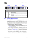
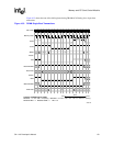
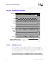
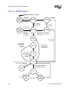
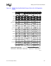
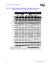
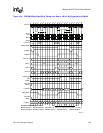
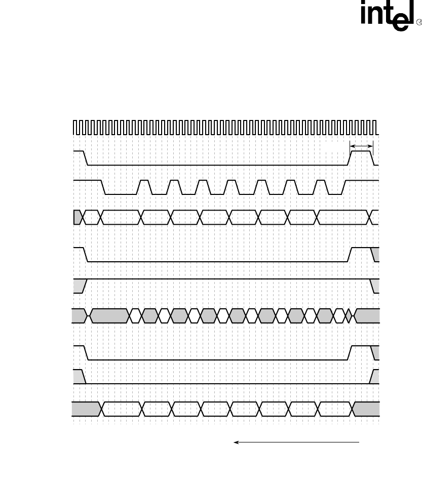
Figure 10-4 shows the rate of the shift registers during FPM or EDO DRAM nCAS timing for
burst-of-eight transactions.
Figure 10-4. Dram Burst-of-Eight Transactions
10.5.3 SDRAM Overview
The SA-1110 supports most x4, x8, x16, and x32 SDRAM. There are fifteen multiplexed
row/column address signals (DRA14-0), four command select signals (nRAS/nSDCS[3:0]), four
data qualifiers for byte selection (nCAS/DQM[3:0]), thirty-two data signals (D[31:0]), a write
enable signal (nWE), a row address strobe (nSDRAS), a column address strobe (nSDCAS), two
memory clocks (SDCLK[2:1]), and a memory clock enable (SDCKE 1).
Whenever an SDRAM bank is enabled, a mode register set (MRS) command is sent to the SDRAM
devices. MRS commands always configure SDRAM internal mode registers for sequential (or
linear) burst type and a burst length of one, while the CAS latency is determined by the TDL0 or
A6634-02
Memory Clock
ADDR
Read Data
Reads:
nRAS
nOE
Read RD/nWR
Writes:
Write Data
Write RD/nWR
nWE
nCAS
COL
D0 D1 D2 D3 D4 D5 D6 D7
COL+4 COL+8
COL+12 COL+16 COL+20 COL+24
COL+28
D0 D1 D2 D3 D4 D5 D6 D7
Row
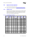
Contents of DRAM register fields:
MDCAS01 = 11 0001 1000 1100 (binary) MDCAS00 = 0110 0011 0001 1000 1100 0110 0000 0111 (binary)
MDCNFG: TRP0 = 4 MDCNFG: CDB20 = 1 TDL0 = 00
TRP+1
firstlast
time