SA-1110 Developer’s Manual 355
Peripheral Control Module
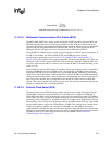
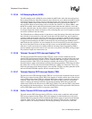
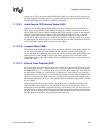
11.12.4 MCP Control Register 1
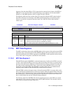
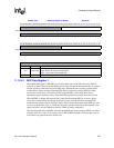
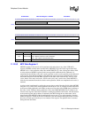
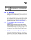
The MCP control register 1 (MCCR1) contains one bit that selects one of two fixed frequencies to
drive the MCP. Note that this register resides within the PPC’s address space.
11.12.4.1 Clock Frequency Select (CFS)
When the on-chip clock is enabled (ECS=0), the clock frequency select (CFS) bit is used to select
either a 9.585-MHz or an 11.981-MHz clock to drive the MCP’s serial clock rate. When ECS=0
and CFS=0, the on-chip 3.6864-MHz oscillator is first multiplied by 13 then divided by 4, resulting
in an 11.9808-MHz bit clock frequency. When ECS=0 and CFS=1, the on-chip 3.6864 MHz
oscillator is first multiplied by 13 then divided by 5, resulting in a 9.58464-MHz bit clock
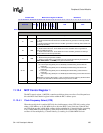
21 ATE
Audio transmit FIFO interrupt enable.
0 – Audio transmit FIFO half-full or less condition does not generate an interrupt (ATS bit
ignored).
1 – Audio transmit FIFO half-full or less condition generates an interrupt (state of ATS sent
to interrupt controller).
22 ARE
Audio receive FIFO interrupt enable.
0 – Audio receive FIFO one- to two-thirds full or more condition does not generate an
interrupt (ARS bit ignored).
1 – Audio receive FIFO one- to two-thirds full or more condition generates an interrupt
(state of ARS sent to interrupt controller).
23 LBM
Loopback mode.
0 – Normal serial port operation enabled.
1 – Output of serial shifter is connected to input of serial shifter internally and control of
TXD4, RXD4, SCLK, and SFRM pins is given to the PPC unit.
25..24 ECP
External clock prescaler.
00 – Clock input using GPIO pin 21 is divided by one before being used to drive the
frame rate.
01 – Clock input using GPIO pin 21 is divided by two before being used to drive the
frame rate.
10 – Clock input using GPIO pin 21 is divided by three before being used to drive the
frame rate.
11 – Clock input using GPIO pin 21 is divided by four before being used to drive the frame
rate.
Note: ECP is used only when ECS=1. Also, the maximum clock frequency allowed to drive
the frame rate after ECS has divided down the input clock is 12 MHz.
31..26 — Reserved.
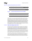
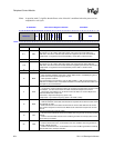
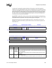
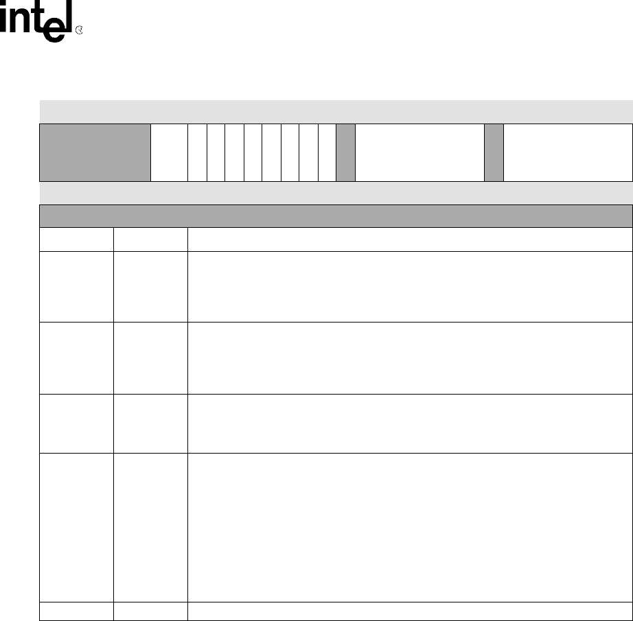
0h 8006 0000 MCP Control Register 0: MCCR0 Read/Write
31 30 29 28 27 26 25 24 23 22 21 20 19 18 17 16 15 14 13 12 11 10 9 8 7 6 5 4 3 2 1 0
Reserved ECP
LBM
ARE
ATE
TRE
TTE
ADM
ECS
MCE
Reserved
TSD
Reserved
ASD
Reset
0 0 0 0 0 0 0 0 ? ? ? ? ? ? ? 0 0 ? ? ? ? ? ? ? 0 ? ? ? ? ? ? ?
(Sheet 2 of 2)
Bits Name Description


