


150 SA-1110 Developer’s Manual
Memory and PC-Card Control Module
but there will be holes in the memory map because the system ignores the still significant internal
address bit IA9. When configured for a 16-bit data bus, 9 column address bits must be used to
avoid memory map holes: this prohibits the use of x16 organized 16Mbit and 64Mbit SDRAM on
16-bit data busses.
10.5.2 DRAM Timing
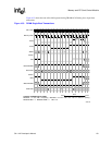
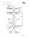
The DRAM nCAS/DQM timing is generated using rotate registers. The rate at which these rotate
registers are clocked is determined by MDCNFG:CDB20,2 and MDCNFG:DWID0,2. The time at
which to sample the read data is programmable to coincide with the deassertion of nCAS/DQM or
up to 3 CPU cycles later. This method provides a way to take advantage of the EDO DRAM while
still supporting the FPM DRAM. A full burst nCAS/DQM waveform is specified, and the memory
interface controller rotates the waveform rotate register once every CPU clock cycle (if
CDB20,2=0 and DWID0,2=0) or once every 2 CPU clock cycles (if CDB20,2=1 or DWID0,2=1).
The rotating continues until the number of nCAS/DQM pulses have been generated that
corresponds to the actual number of data words being accessed.
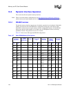
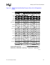
Register set MDCAS00/MDCAS01/MDCAS02 or MDCAS20/MDCAS21/MDCAS22 are
programmed to contain the nCAS/DQM waveform for a full burst access (8-beat for 32-bit data
busses and 16-beat for 16-bit data busses). To begin an access, the row address is output on
DRA[14:0], which is A[24:10]. One CPU clock later (one-half memory clock), nRAS/nSDCS is
asserted and the nCAS/DQM waveform begins and is rotated with each CPU clock, if CDB20,2=0
and DWID0,2=0. A "1" in these rotate registers drives nCAS/DQM high (deasserts) at the rising
edge of the CPU clock cycle, and a "0" drives nCAS/DQM low (asserts). The column address for
the first beat of data will be valid 1 CPU cycle before nCAS/DQM transitions from deasserted to
asserted. During reads, a rising edge is detected on the nCAS/DQM waveform and input data is
latched MDCNFG:TDL0, 2 cycles after the rising edge. The rotate register continues to rotate until
the number of nCAS/DQM pulses equals the burst size of the current transaction. For writes,
nRAS/nSDCS will be deasserted on the next rising memory clock cycle edge after the last
nCAS/DQM rising edge (either 1 or 2 CPU clock cycles). For reads, nRAS/nSDCS will be
deasserted on the rising memory clock cycle edge that occurs 2 or 3 CPU clock cycles after the
input data is latched. For each additional beat after the first, the column address will be updated
coincident with the deassertion of nCAS/DQM, or 1 CPU cycle later. For writes, the write data
outputs will follow the same timing as the column address. nWE and nOE, as appropriate, follow
the same timing as nRAS/nSDCS. After nRAS/nSDCS is deasserted, the timing parameter
MDCNFG:TRP0,2 is used to determine the wait before the next assertion of nRAS/nSDCS.
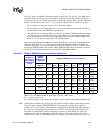
If CDB20,2=1 or DWID0,2=1, the nCAS/DQM waveform will be rotated every memory clock, or
every 2 CPU cycles. The timing of the other signals remains the same relative to the nCAS/DQM
waveform. For CDB20,2=0 and DWID0,2=0, there is a requirement that nCAS/DQM high and low
times be programmed with a minimum of 2 bits and the 4 least significant bits in MDCAS00 and
MDCAS20 must be "1". For CDB20,2=1 or DWID0,2=1, the high and low nCAS/DQM pulse
times may be 1 bit each and the least significant 2 bits of MDCAS00 or MDCAS20 must be "1".
These requirements are necessary for the internal hardware to properly generate addresses and
write data and for proper address and data setup times.