


292 SA-1110 Developer’s Manual
Peripheral Control Module
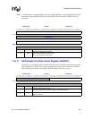
11.8.12 UDC Data Register (UDCDR)
UDCDR is an 8–bit register corresponding to both the top and bottom entries of the Transmit FIFO
and Receive FIFOs, respectively. The SA-1110 UDC’s receive logic places data into the top of the
Receive FIFO. The data is transferred down the FIFO to the lowest location that is empty. When
UDCDR is read, the bottom entry of the Receive FIFO is accessed. After the read, the bottom FIFO
entry is invalidated and all FIFO data automatically transfers down one byte location.
When UDCDR is written, the topmost entry of the Transmit FIFO is accessed. After a write, the
data is automatically transferred down the Transmit FIFO to the lowest available location. The
SA-1110 UDC’s transmit logic:
• acquires 8-bit data values from the bottom of the Transmit FIFO, one byte at a time
• places the data into a serial shifter
• transmits the data to the Host via the SA-1110 UDC pins
Each time a data value is taken from the bottom of the Transmit FIFO, the location is invalidated
and all remaining data in the Transmit FIFO is automatically transferred down one location.
The following table shows the location of the top and bottom of the Transmit and Receive FIFOs in
UDCDR. Both the Transmit FIFO and Receive FIFO are cleared when the SA-1110 is reset or
when the UDD bit in UDCCR is written to one. After either of these actions take place, and before
the SA-1110 UDC is enabled, the Transmit FIFO must be “primed” by writing up to sixteen 8-bit
values to UDCDR.
11.8.13 UDC Status/Interrupt Register (UDCSR)
UDCSR contains six bits that are used to generate the SA-1110 UDC’s interrupt request. Each bit
in UDCSR is logically ORed together to produce one interrupt request. When the Interrupt Service
Routine (ISR) for the SA-1110 UDC is executed, it must read UDCSR to determine which interrupt
request occurred.
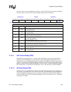
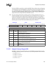
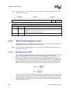
0h 8000 0028 UDCDR Read/Write
7 6 5 4 3 2 1 0
Bottom of Receive FIFO
Reset
? ? ? ? ? ? ? ?
Read Access
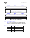
7 6 5 4 3 2 1 0
Top of Transmit FIFO
Reset
? ? ? ? ? ? ? ?
Write Access
Bits Name Description
7..0 DATA
Top/bottom of transmit/receive FIFO data.
Read – Bottom of receive FIFO data.
Write – Top of transmit FIFO data.