


180 SA-1110 Developer’s Manual
Memory and PC-Card Control Module
10.7.2 External Logic for PC-Card Implementation
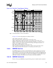
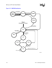
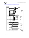
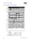
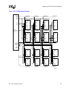
The SA-1110 requires external logic to complete the PC-Card socket interface. Figure 10-20 and
Figure 10-21 show general solutions for a two– and one–socket configuration. GPIO or
memory-mapped external registers are used to control the PC-Card interface’s reset, power
selection (VCC and VPP), and driver enable lines. For dual–voltage support, level shifting buffers
are required for all SA-1110 input signals. Each figure shows the logical connections necessary to
support hot insertion capability. Hot insertion capability requires the sockets to be electrically
isolated from each other and from the remainder of the memory system.
Note: If one or both of these features (hot insertion and dual–voltage) is not required, then the logic
related to the feature which is not required may be eliminated.
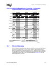
The pull-ups shown are included for compliance with PC Card Standard - Volume 2 - Electrical
Specification. For low-power systems, it is recommended to remove power from these pull-ups
during sleep to avoid unnecessary power consumption. The CD1# and CD2# signals have been
“OR’ed” before being provided to the SA-1110. This signal is then routed into a GPIO pin for
interrupt capability. Similarly, RDY/BSY# is routed to a GPIO pin. The INPACK# signal is not
used. In the data bus transceiver control logic, it is recommended that nPCE1 control the enable for
the low byte lane and nPCE2 control the enable for the high byte lane.