


330 SA-1110 Developer’s Manual
Peripheral Control Module
11.11.4 UART Control Registers 1 and 2
UART control register 1 (UTCR1) contains the upper 4 bits and UTCR2 the lower 8 bits of the
baud rate divisor field.
11.11.4.1 Baud Rate Divisor (BRD)
The 12-bit baud rate divisor (BRD) field is used to select the baud or bit rate of the UART. A total
of 4096 different baud rates can be selected, ranging from a minimum of 56.25 bps to a maximum
of 230.4 Kb/ps. The baud rate generator uses the 3.6864-MHz clock generated by the on-chip PLL
divided by 16 to generate the bit clock. A digital PLL is used to synchronize the baud rate of the
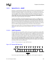
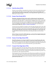
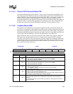
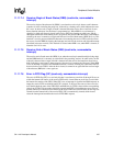
0h 8005 0000 UTCR0 Read/Write
7 6 5 4 3 2 1 0
Reserved TCE RCE SCE DSS SBS OES
PE
Reset
0 ? ? ? ? ? ? ?
Bits Name Description
0PE
Parity enable.
0 – Parity checking on received data and parity generation on transmitted data is disabled.
1 – Parity checking on received data and parity generation on transmitted data is enabled.
1OES
Odd/even parity select.
0 – Odd parity checking/generation selected. Parity error bit set if even number of ones
counted in data field (including the parity bit).
1 – Even parity checking/generation selected. Parity error bit set if odd number of ones
counted in data field (including the parity bit).
2SBS
Stop bit select.
0 – One stop bit transmitted per frame.
1 – Two stop bits transmitted per frame.
Note: Receiver not affected by SBS; always checks for one stop bit.
3DSS
Data size select.
0 – 7-bit data.
1 – 8-bit data.
Note: For 7-bit mode, the data is right justified within the FIFO entries, the MSBs in the
receive FIFO are zero filled, and the MSBs in the transmit FIFO are ignored.
4SCE
Sample clock enable.
0 – on-chip baud rate generator and digital PLL used to transmit and receive asynchronous
data.
1 – A clock is input via GPIO pin 20 and is used synchronously to sample receive data and
drive transmit data.
Note: Serial port 1’s UART uses GPIO pin 18 for the sample clock input; serial port 2 does
not support the sample clock function. The user must also program the appropriate bits in
the GPDR and GAFR registers within the system control module.
5 RCE
Receive clock edge select.
0 – Rising edge of clock input on GPIO pin 20 used to latch data from the receive pin if SCE=1.
1 – Falling edge of clock input on GPIO pin 20 used to latch data from the receive pin if SCE=1.
6TCE
Transmit clock edge select.
0 – Rising edge of clock input on GPIO pin 20 used to drive data onto the transmit pin if SCE=1.
1 – Falling edge of clock input on GPIO pin 20 used to drive data onto the transmit pin if SCE=1.
7 — Reserved.