


SA-1110 Developer’s Manual 347
Peripheral Control Module
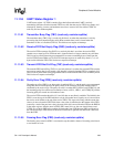
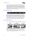
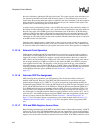
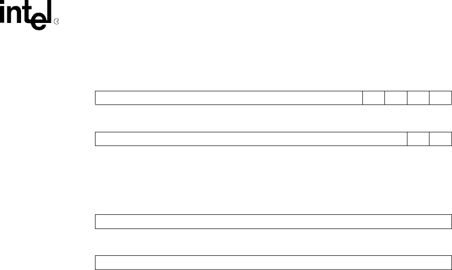
Figure 11-31. Audio/Telecom Receive Data Format From UDC1x00
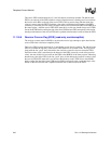
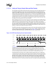
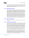
Figure 0-5. Audio/Telecom Receive Data Format From 16-bit CODECs
To reduce chip size as well as power consumption, the MCP’s FIFOs use self-timed logic (not
clocked). Because of process and environmental variations, the depth at which a service request is
triggered to empty the receive FIFOs is variable. This variation spans a maximum of four FIFO
entries, thus the audio and telecom receive FIFO service requests can be made at four different
FIFO depths.To compensate for this variability and guarantee that at least four valid entries of data
exist within either FIFO before generating a service request, an extra four entries have been added
to both receive FIFOs (four entries more than the transmit FIFOs). Thus the audio and telecom
transmit FIFOs are 8-entries deep and the audio and telecom receive FIFOs are 12-entries deep.
The point at which the receive FIFO service requests are triggered spans one-third (four entries) of
the 12-entry FIFOs. The service request is signalled at a depth from one-third full to two-thirds full
(when the FIFOs contains five, six, seven, or eight entries of data).
11.12.1.4 Codec Control Register Data Transfer
The UCB1100, UCB1200, and UCB1300 contain sixteen 16-bit registers used to configure the
chip, and store touch-screen and ADC samples as well as digital I/O pin state and edge interrupt
status. These registers are read and written via the MCP’s serial interface using three fields that
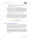
exist within the MCP’s data frame. In Figure 11-28, bits [15:0] contain the value read from or
written to the off-chip codec, bits [46:43] contain the register address of the current read or write,
and bit 42 is used by the MCP to signal a read or write cycle to the codec. These fields are
configured by the CPU by writing to MCP data register 2, and are then transmitted to the off-chip
codec. These fields are also received every data frame by the MCP from the codec and are placed
in MCP control register 2, which can be read by the CPU. Note that the contents of the addressed
register are returned in the receive data frame regardless of the state of the read/write bit. Thus for
write cycles, both a write and a read occurs, and for read cycles, only a read occurs.
A register write is performed by writing a value to the MCP data register 2 that contains the value
to store to the register, the address of the register, and the read/write bit set to one. Once this
register is written, its contents are transferred to the correct fields within the serial shifter on the
next rising edge of the SFRM signal. The register information is transmitted to the UCB1100,
UCB1200, or UCB1300 during subframe 0, and the value is written to the selected codec register at
Bit1514131211109876543210
Audio Data 0 0 0 0
Bit1514131211109876543210
Telecom D ata 0 0
Bit1514131211109876543210
Audio Data
Bit1514131211109876543210
Telecom Data