


138 SA-1110 Developer’s Manual
Memory and PC-Card Control Module
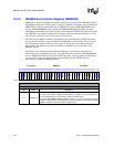
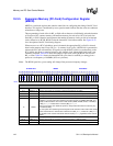
Sharing MDCAS Registers
Asynchronous DRAM or SDRAM can share MDCAS registers with SMROM. Asynchronous
DRAM must use CDB2n=1 and/or the CPU clock period (labeled "Tcpu" in Table 10-4)mustbe
fairly large. SDRAM and SMROM can share MDCAS registers if they use the same RAS-to-CAS
delay (the entries labeled “trcd” in Table 10-4). If both the SDRAM and SMROM use the memory
clock frequency, they must also use the same clock edge for read data latching.
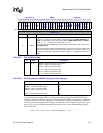
MDCAS registers can be shared even if the SDRAM and SMROM are running at different
frequencies (For example, SMROM using SDCLK 0 with MDREFR:K0DB2=1 and SDRAM using
SDCLK 1 with MDREFR:K1DB2=0). This is possible because the minimum number of clock
cycles for RAS-to-CAS delay typically scales with frequency.
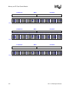
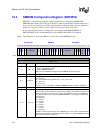
Reference edges for CAS latency are made insensitive to the clock divisor by ignoring
odd-numbered (first, third, and so forth) "0" to "1" transitions if MDREFR:K0DB2=1 for
SMROM, MDREFR:K1DB2=1 for SDRAM bank pair 0/1, or MDREFR:K2DB2=1 for SDRAM
bank pair 2/3). The number of “0” to “1” transitions required to serve a burst transaction becomes
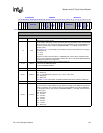
twice the burst length. By repeating the pattern of “0” to “1” transitions up through the most
significant bit of MDCAS, one can ensure that an internal burst length of eight will always be
accommodated: even if the transaction uses a 16-bit data bus (SDRAM, but not SMROM) and the
memory clock divisor.