


SA-1110 Developer’s Manual 385
Peripheral Control Module
11.13.4 PPC Pin State Register
Pin state is both monitored and controlled by reading/writing the PPC pin state register (PPSR). The
PPSR contains 1 state bit for each of the 22 peripheral pins. This register may be read at any time to
determine the current state of all peripheral pins, even when pins are controlled by the peripheral
rather than the PPC. If a peripheral is disabled and its corresponding pin direction is programmed as
an output in the PPDR, its PPSR bit is used to control the state of the peripheral pin. Writing a zero to
the pin’s state bit causes the pin to be forced low, and writing a one causes the pin to be forced high.
Writing a value to a pin state bit that is an input or is not under the control of the PPC has no effect. To
alter the state of an output pin, the user should first read the PPSR, then logically AND the value read
with a mask, which contains ones in every bit position except the one the user wishes to clear. To set a
pin, the user should logically OR the value read with a mask, which contains zeros in every bit
position except the one the user wishes to set. This mechanism allows the user to set or clear
individual pins without changing the state of other pins that are configured as outputs.
Serial port 2 contains two bits that control the polarity of data input via the receive pin (RXD2) and
data output via the transmit pin (TXD2). The user must ensure that these polarity bits are set
(RXP = TXP = 1), which selects true or noninverted data before using TXD2 or RXD2 as GPIO
pins.
Note that PPSR is implemented as two separate registers. A write to PPSR addresses one of the
registers and is used to set and clear pins configured as GPIO outputs, while a read addresses the
other register that is used to store and monitor pin state. The register used to store pin state contains
logic to synchronize the signal input from the pin to allow the user to read it. The pins are sampled
at a rate of 7.3728 MHz; each synchronization cycle takes 135.6 ns. Depending on the CPU
frequency programmed by the user, after changing the state of an output pin via a write, one or
more dummy read cycle waitstates may need to be inserted to allow the value to be output to the
pin and to allow the synchronizer to resample the pin.
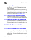
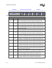
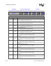
The following table shows the location of each pin state bit and to which peripheral pin it
corresponds
. Note that this register is not reset and that for reserved bits, writes are ignored and
reads return one.
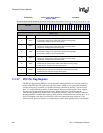
20 SCLK
Serial port 4: MPC/SSP serial clock pin direction.
0 – If serial port 4 disabled, serial clock pin configured as general-purpose input.
1 – If serial port 4 disabled, serial clock pin configured as general-purpose output.
21 SFRM
Serial port 4: MPC/SSP serial frame pin direction.
0 – If serial port 4 disabled, serial frame pin configured as general-purpose input.
1 – If serial port 4 disabled, serial frame pin configured as general-purpose output.
31..22 — Reserved.
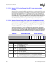
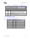
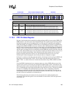
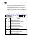
0h 9006 0000 PPC Pin Direction Register: PPDR Read/Write
31 30 29 28 27 26 25 24 23 22 21 20 19 18 17 16 15 14 13 12 11 10 9 8 7 6 5 4 3 2 1 0
Reserved
SFRM
SCLK
RXD4
TXD4
RXD3
TXD3
RXD2
TXD2
RXD1
TXD1
L_BIAS
L_FCLK
L_LCLK
L_PCLK
LDD 7
LDD 6
LDD 5
LDD 4
LDD 3
LDD 2
LDD 1
LDD 0
Reset 1 1 1 1 1 1 1 1 1 1 0 0 0 0 0 0 0 0 0 0 0 0 0 0 0 0 0 0 0 0 0 0
(Sheet 2 of 2)
Bits Name Description