


SA-1110 Developer’s Manual 351
Peripheral Control Module
11.12.3.3 Multimedia Communications Port Enable (MCE)
The MCP enable (MCE) bit is used to enable and disable all MCP operation. Since the MCP and
SSP both share the same pins, only one can be enabled at a time. If the user enables both at the
same time, the MCP has precedence and the SSP remains disabled. However, both can be enabled
when the SSP pin reassignment (SPR) bit within the PPC unit is set, which assigns the SSP to
GPIO pins. See the following sections for a description of the SSP enable (SSE) bit.
When the MCP is disabled, all of its clocks are powered down to minimize power consumption. If
the SSP is also disabled, the TXD4, RXD4, SCLK, and SFRM pins can be used for
general-purpose input/output. See the Section 11.13, “Peripheral Pin Controller (PPC)” on
page 11-382 for a description of how to program the PPC unit to reassign the SSP’s pins and to use
serial port 4’s pins as I/Os. Note that MCE and CFS are the only control bits within the MCP that
are reset to a known state. MCE is cleared to zero to ensure the MCP is disabled following a reset
of the SA-1110.
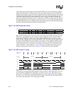
When the MCP is enabled, SCLK begins to transition and the start of the first frame is signalled by
pulsing the SFRM pin high for one SCLK period. The rising edge of SFRM coincides with the
rising edge of SCLK. As long as the MCE bit is set, the MCP operates continuously, transmitting
and receiving 128 bit data frames. When the MCE bit is cleared, the MCP is disabled immediately,
causing the current frame, which is being transmitted, to be terminated and control of serial port 4’s
pins to be given to the PPC unit. Clearing MCE resets the MCP’s FIFOs. However, MCP data
register 3, the control, and the status registers are not reset. The user must ensure these registers are
properly reconfigured before re-enabling the MCP.
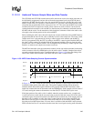
11.12.3.4 External Clock Select (ECS)
The external clock select (ECS) bit selects whether one of the two on-chip clocks derived by the
3.6864-MHz oscillator is used by the MCP or if an off-chip clock is supplied via GPIO pin 21.
When ECS=0, the MCP can be programmed to select one of two frequencies: either 9.585 MHz or
11.981 MHz. This clock is also used to increment the audio and telecom sample rate counters. (See
preceding sections.) When ECS=1, the MCP uses GPIO 21 to input a clock supplied from off-chip.
The frequency of the off-chip clock after being scaled by the ECP bit field can be any value within
the allowable frequency range of the UCB1x00 up to 12 MHz. This off-chip clock is useful when a
sample rate frequency, which is not a multiple of 9.585 MHz or 11.981 MHz is required for
synchronization with either the audio and/or telecom portion of the UCB1x00 codecs. When using
GPIO pin 21 for the input clock, the user must also set bit 21 of the GPIO alternate function register
(GAFR) and clear bit 21 of the GPIO pin direction register (GPDR). See the Section 9.1,
“General-Purpose I/O” on page 9-73.
SampleRate
Freq
32xTSD
-----------------------=
Valid ASD values are from 4 (00000100) to 127 (11111111)