


SA-1110 Developer’s Manual 349
Peripheral Control Module
to service the transmit and/or receive FIFOs, the user must ensure the DMA is properly configured
to perform half-word accesses, using 4 half-words per burst (half the size of the FIFOs). Note that a
separate set of registers also exist to configure SSP operation. See the following sections for a full
description of programming and operation of serial port 4 as an SSP, a summary of serial port 4’s
MCP registers, and a summary of its SSP registers.
11.12.2 MCP Register Definitions
There are six registers within the MCP: two control registers, three data registers, and one status
register. The control register is used to program the audio and telecom sample rates, to mask or
unmask interrupt requests to service the MCP’s FIFOs, to select whether an on-chip or off-chip clock
is used to drive the bit rate, and to enable/disable operation. The first data register addresses the top of
the audio transmit FIFO and the bottom of the audio receive FIFO. Likewise, the second data register
addresses the top/bottom of the telecom transmit/receive FIFOs, respectively. A read accesses the
receive FIFOs; a write accesses the transmit FIFOs. Note that these are four physically separate
FIFOs to allow full-duplex transmission. The third data register is used to transmit read and write
operations to the codec’s control, data, and status registers. Values written to the register are used in
the transmit data frame and values read from the register are taken from the received data frame. The
status register contains bits that signal FIFO overrun and underrun errors, and transmit and receive
FIFO service requests. Each of these status conditions signals an interrupt request to the interrupt
controller. The status register also flags when audio and telecom transmit FIFOs are not full, when the
audio and telecom receive FIFOs are not empty, when a codec control register read or write is
complete, and when the audio or telecom portion of the codec is enabled (no interrupt generated).
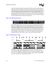
11.12.3 MCP Control Register 0
The MCP control register (MCCR0) contains 11 different bit fields that control various functions
within the MCP.
11.12.3.1 Audio Sample Rate Divisor (ASD)
The 7-bit audio sample rate divisor (ASD) bit field is used to synchronize the MCP with the sample
rate of the audio codec. Sample rate synchronization is required such that the MCP’s audio transmit
FIFO logic knows when to load a new value for D-to-A conversion to the MCP’s serial shifter for
transmission. This field is programmed with the same value that is written to the codec’s sample
rate divisor via a codec control register write. When the audio codec is enabled, the first audio
transmit value is placed in the serial output stream by the transmit FIFO, and both the MCP’s and
codec’s sample rate counters begin to decrement in lock-step with one another. When the audio
codec’s counter decrements to zero, it uses the value transmitted to it by the MCP to perform the
D-to-A conversion. After the conversion is made, the MCP and codec’s counters reset to their
modulus values, and the MCP’s audio transmit FIFO loads the next value to the serial shifter for
transmission. This new value is then transmitted to the audio codec and is used for the next D-to-A
conversion, which is signalled when the sample rate counter decrements to zero again.
A total of 123 different audio sample rates can be selected, ranging from a minimum of 2.36 K
samples per second using the 9.585-MHz internal clock to a maximum of 93.59 K samples per
second using the 11.981-MHz internal clock. Note that slower sample rates can be achieved using
an externally supplied clock. The sample rate clock generator uses either a 9.585-MHz or
11.981-MHz clock produced by the on-chip PLL or the clock supplied to the MCP via GPIO pin
21, and is divided by a fixed value of 32 and then by the programmable ASD value to generate the
audio sample clock. This sample clock is automatically enabled when: