


SA-1110 Developer’s Manual 329
Peripheral Control Module
11.11.3.4 Data Size Select (DSS)
The data size select (DSS) bit is programmed to select the size of the data transmitted and received
within each frame. Data can be 7 or 8 bits in length. When 7-bit data is programmed, the data is
right justified within the FIFOs. The unused bit is zero filled within the receive FIFO, and is
ignored within the transmit FIFO. Note that the user must right justify data supplied to the transmit
FIFO when 7-bit data is selected.
11.11.3.5 Sample Clock Enable (SCE)
The sample clock enable (SCE) bit is used to enable or disable the use of a clock input from a
GPIO pin to synchronously sample and drive data to and from the UART. When SCE=0, the
on-chip 3.6864-MHz PLL, the UART’s programmable baud rate generator, and the receive logic’s
digital PLL are used. When SCE=1, a clock is input from a GPIO pin and is used to synchronously
drive both the transmit and receive logic. Note that the user must configure the GPIO pin as an
input by clearing the corresponding bit in the GPIO pin direction register (GPDR) and switch
control of the GPIO pin to the UART by setting the corresponding bit in the GPIO alternate
function register (GAFR). See Chapter 9, “System Control Module”.
For the receive logic, the RCE bit is decoded to select which edge of the input clock is used to latch
each bit of the incoming frame. Note that the clock is not embedded within the data stream and the
digital PLL is shut down to conserve power. For the transmit logic, the TCE bit is decoded to select
which edge of the input clock is used to drive each bit of the outgoing frame. Note that the clock
driving the programmable baud rate generator is shut down when SCE=1 to conserve power. Also
note that SCE does not affect the frame format of data being transmitted and received by the
UART.
The SA-1110 has a total of three UARTs (serial ports 1, 2 and 3). When the external sample clock
function is enabled, serial port 1 uses the GPIO 18 pin and serial port 3 uses GPIO 20. Serial port 2
does not support the sample clock function.
11.11.3.6 Receive Clock Edge Select (RCE)
When SCE=1, the receive clock edge select (RCE) bit is used to select which edge of the clock
input from the GPIO pin to use (rising or falling) to synchronously sample data from the receive
pin. When RCE=0, each bit received is sampled on the rising edge of the sample input clock; when
RCE=1, bits are sampled on the clock’s falling edge. Note that the internal baud rate generator and
receive logic’s digital PLL are not used in this mode. RCE is ignored when SCE=0.
11.11.3.7 Transmit Clock Edge Select (TCE)
When SCE=1, the transmit clock edge select (TCE) bit is used to select which edge of the clock
input from the GPIO pin to use (rising or falling) to synchronously drive data onto the transmit pin.
When TCE=0, each bit transmitted is driven on the rising edge of the sample input clock; when
TCE=1, bits are driven on the clock’s falling edge. Note that the internal baud rate generator is not
used in this mode. TCE is ignored when SCE=0.
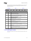
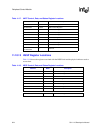
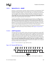
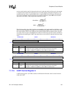
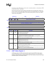
The following table shows the bit locations corresponding to the seven different control bit fields
within UART control register 0. The UART must be disabled (RXE=TXE=0) when changing the
state of any bit within this register. The reset state of these control bits is unknown (indicated by
question marks) and must be initialized before enabling the UART. Note that writes to bit 7 are
ignored and reads return zero.