


356 SA-1110 Developer’s Manual
Peripheral Control Module
frequency. Note that when ECS=1, CFS is ignored and an external clock is input to the MCP via
GPIO pin 21. Also note that CFS is cleared following a reset of the SA-1110 so that the MCP
defaults to 11.981-MHz operation, which is standard for the UCB1x00.
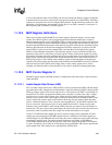
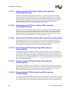
The following table shows the location of the CFS control bit within the MCP control register 1.
The CFS is cleared to zero selecting 11.981-MHz operation following a reset of the SA-1110.
Writes to reserved bits are ignored and reads return zeros. MCCR1 resides within the PPC’s
address space.
11.12.5 MCP Data Registers
The MCP contains three data registers. MCDR0 addresses the top entry of the audio transmit FIFO
and bottom entry of the audio receive FIFO, MCDR1 addresses the top and bottom entries of the
telecom transmit and receive FIFOs respectively, and MCDR2 is used to perform reads and writes
to any of the codec’s 16 registers via the MCP’s serial interface.
11.12.5.1 MCP Data Register 0
When MCP data register 0 (MCDR0) is read, the bottom entry of audio receive FIFO is accessed.
As data is removed by the MCP’s receive logic from the incoming data frame, it is placed into the
top entry of the audio receive FIFO and is transferred down an entry at a time until it reaches the
last empty location within the FIFO. Data is removed by reading MCDR0, which accesses the
bottom entry of the audio FIFO. After MCDR0 is read, the bottom entry is invalidated and all
remaining values within the FIFO automatically transfer down one location.
When MCDR0 is written, the topmost entry of the audio transmit FIFO is accessed. After a write,
data is automatically transferred down to the lowest location within the transmit FIFO, which does
not already contain valid data. Data is removed from the bottom of the FIFO one value at a time by
the transmit logic, is loaded into the correct position within the 64-bit transmit serial shifter, and
then is serially shifted out onto the TXD4 pin during subframe 0.
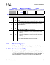
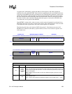
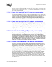
The following table shows MCDR0. Note that the transmit and receive audio FIFOs are cleared
when the SA-1110 is reset or by writing a zero to MCE (MCP disabled). Also note that writes to
reserved bits are ignored and reads return zeros.
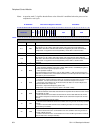
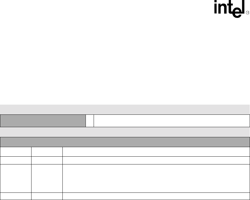
0h 9006 0030 MCP Control Register 1: MCCR1 Read/Write
31 30 29 28 27 26 25 24 23 22 21 20 19 18 17 16 15 14 13 12 11 10 9 8 7 6 5 4 3 2 1 0
Reserved
CFS
Reserved
0 0 0 0 0 0 0 0 0 0 0 0 0 0 0 0 0 0 0 0 0 0 0 0 0 0 0 0 0 0 0 0
Bits Name Description
19..0 — Reserved.
20 CFS
Clock frequency select.
0 – If ECS=0, bit rate clock frequency of 11.981 MHz is selected.
1 – If ECS=0, bit rate clock frequency of 9.585 MHz is selected.
If ECS=1, CFS is ignored and an external clock supplied by GPIO pin 21 is used.
31..21 — Reserved.