


172 SA-1110 Developer’s Manual
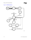
Memory and PC-Card Control Module
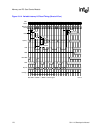
10.6.7 FLASH Memory Interface Overview
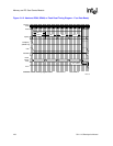
The SA-1110 provides an SRAM-like interface for access of Flash memory. The RDF fields in the
MSCx registers are the latency for each read access to nonburst Flash or the first read access to
burst Flash; it also controls the nWE assertion time during a write cycle (nonburst) to burst Flash.
The RDN field controls subsequent read access times to burst Flash and the nWE low time during a
write cycle to nonburst Flash. RRR is the time from nCS deassertion after a read to the start of a
read from a different memory or after a write to another memory access. A single DRAM CBR
refresh cycle may be inserted between words of a burst read from Flash memory. During the
refresh cycle, nCS and nOE are deasserted.
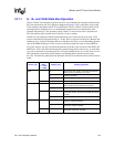
There are some requirements for writes to Flash memory:
• Flash memory write space must be uncacheable and unbuffered.
• Writes to Flash memory must be exactly the width of the populated Flash devices on the data
bus (for examples, byte writes to a 32-bit bus or word writes to a 16-bit bus are not permitted).
• Software is responsible for partitioning commands and data, and writing these to Flash
memory in the appropriate sequence
A single CBR refresh cycle, for asynchronous DRAM and/or SDRAM, may be inserted between
word accesses within a burst read. nCS and nOE are deasserted during the refresh cycle.
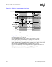
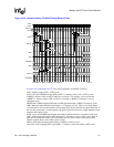
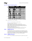
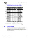
10.6.8 FLASH Memory Timing Diagrams and Parameters
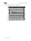
Nonburst Flash reads have the same timing as nonburst ROMs as shown in the preceding figures.
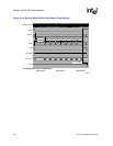
Figure 10-16 shows the timing for writes to nonburst Flash. Writes to burst Flash use nonburst
accesses and equivalent timings, except the nWE assertion time and data setup use RDF+1 instead
of RDN+1.