


388 SA-1110 Developer’s Manual
Peripheral Control Module
The following table shows the location of the two pin reassignment bits. Note that for reserved bits,
writes are ignored and reads return zero. Both control bits are cleared to one following a reset of the
SA-1110, giving control of all GPIO pins to the system control module.
11.13.6 PPC Sleep Mode Pin Direction Register
When sleep mode is entered, reset is asserted to all of the SA-1110’s peripherals and to the PPC unit.
The PPC pin direction register is cleared during a hard, soft, or sleep reset, causing the peripheral pins
under the PPC’s control to be configured as inputs. If this register were also used to determine pin
direction during sleep, the pins would all be configured as inputs. This action would cause any off-chip
device that expects data to be output from the SA-1110 to burn power during sleep because its input
would float. The sleep mode pin direction register (PSDR) prevents this undesired power consumption
by allowing the user to establish peripheral pin direction during and immediately following sleep mode.
When sleep mode is entered, both the peripherals and the PPC are reset; however, PSDR is not reset
like PPDR. Once the user programs PSDR, it retains its data after sleep mode is entered and reset is
asserted. The power manager uses the values in PSDR to determine the direction and state of the 22
peripheral pins. When a sleep mode direction bit is programmed to a zero, the corresponding pin is
configured as an output and is driven low (zero). If it is programmed to a one, it is an input. The
power manager latches the contents of PSDR before VDD is removed from the SA-1110 to maintain
the peripheral pin direction and state after the main power supply is removed. Once VDD is removed,
the data in PSDR is lost and must be reprogrammed after exiting sleep mode. The power manager
contains a control bit called the peripheral control hold (PSSR:PH). This bit is set upon exit from
sleep mode and indicates that the peripheral pins are being held in their sleep state. Following sleep,
the user should first reprogram the peripherals and the PPC, then clear PH (by writing a one to it) to
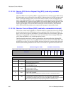
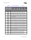
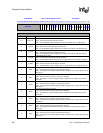
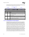
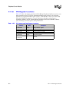
0h 9006 0008
PPC Pin Assignment Register:
PPAR
Read/Write
31 30 29 28 27 26 25 24 23 22 21 20 19 18 17 16 15 14 13 12 11 10 9 8 7 6 5 4 3 2 1 0
Reserved
SPR
Reserved
UPR
Reserved
Reset
1 1 1 1 1 1 1 1 1 1 1 1 1 0 1 1 1 1 1 0 1 1 1 1 1 1 1 1 1 1 1 1
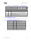
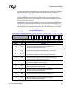
Bits Name Description
11..0 — Reserved.
12 UPR
UART pin reassignment.
0 – No pin reassignment made, GPIO 14-15 controlled by GPIO unit, serial port 1 UART
assigned to TXD1 and RXD1 if SUS=1.
1 – Pin reassignment made, serial port 1 defaults to GPCLK operation (SUS ignored),
UART transmit assigned to GPIO 14 and receive to GPIO 15, GAFR and GPDR must be
configured in GPIO unit.
17..13 — Reserved.
18 SPR
SSP pin reassignment..0 – No pin reassignment made, GPIO 10-13 controlled by GPIO
unit, serial port 4 SSP assigned to TXD4, RXD4, SCLK, and SFRM if MCE=0 and SSE=1.
1– Pin reassignment made, serial port 4 defaults to MCP operation, SSP transmit assigned
to GPIO 10, receive to GPIO 11, serial clock to GPIO 12, and serial frame to GPIO 13,
GAFR and GPDR must be configured in GPIO unit.
31..19 — Reserved.