


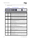

350 SA-1110 Developer’s Manual
Peripheral Control Module
• A MCP data register 2 write to the audio control register B is made (address=0b100), which
sets either the audio codec input or output enable bits (bit 14 = aud_in_ena, bit 15 =
aud_out_ena), followed by
• The rising edge of the next SFRM pulse after the write has been made.
Once enabled, the MCP’s audio sample rate clock decrements at the programmed frequency with a 50%
duty cycle. The action outlined in the above first bullet item causes the MCP’saudio transmit FIFO logic
to transfer the next available value to the audio data field within the serial shifter. Each time the audio
sample rate clock decrements to zero, it is reloaded with its programmed ASD modulus value, triggers
the audio transmit FIFO logic to transfer the next available value to the audio data field within the serial
shifter, and continues to decrement. The MCP’s audio sample rate clock is automatically disabled when:
• A MCP data register 2 write to the audio control register B is made (address=0b100), which
clears both the audio codec input and output enable bits (bit 14 = aud_in_ena, bit 15 =
aud_out_ena), followed by
• The rising edge of the next SFRM pulse after the write has been made.
The resultant audio sample clock rate, given a specific ASD value, can be calculated using the following
equation, where ASD is the decimal equivalent of the binary value programmed within the bit field. Note
that ASD must be programmed with a value of 4 or larger. Unpredictable results occur for ASD values
smaller than 4. Note that one of three clock frequencies can be selected. The first two frequencies are
internal clocks selected by the CFS bit in MCCR1 and the third frequency is a user-defined clock that is
input via GPIO pin 21 and is divided as defined by the ECP bit field described in following sections.
11.12.3.2 Telecom Sample Rate Divisor (TSD)
The 7-bit telecom sample rate divisor (TSD) bit field is used to synchronize the MCP with the
sample rate of the telecom codec. The telecom sample rate clock is required for the same reason
and works exactly like the audio sample rate clock, except for one minor difference. The valid TSD
values range from 4 to 127, allowing a total of 123 different audio sample rates to be selected,
ranging from a minimum of 2.36 K samples per second using the 9.585-MHz internal clock to a
maximum of 93.59 K samples per second using the 11.98-MHz internal clock. Note that slower
sample rates can be achieved using an externally supplied clock.
The resultant telecom sample clock rate, given a specific TSD value, can be calculated using the
following equation, where TSD is the decimal equivalent of the binary value programmed within
the bit field. Note that TSD must be programmed with a value of 4 or larger. Unpredictable results
occur for TSD values smaller than 4. Note that one of three clock frequencies can be selected. The
first two frequencies are internal clocks selected by the CFS bit in MCCR1 and the third frequency
is a user-defined clock that is input via GPIO pin 21 and is divided by the ECP bit field described in
the following sections.
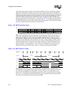
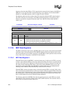
SampleRate
Freq
32xASD
------------------------=
Valid ASD values are from 4 (00000100) to 127 (11111111)