


316 SA-1110 Developer’s Manual
Peripheral Control Module
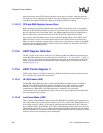
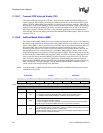
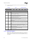
11.10.9 HSSP Data Register
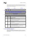
The HSSP data register (HSDR) is an 8-bit register corresponding to both the top and bottom entry
of the transmit and receive FIFOs, respectively.
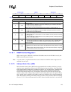
When HSDR is read, the lower 8 bits of the bottom entry of the 11-bit receive FIFO is accessed. As
data enters the top of the receive FIFO, bits 8 – 10 are used as tags to indicate various conditions
that occur during reception of each piece of data. The tag bits are transferred down the FIFO along
with the data byte that encountered the condition. When data reaches the bottom, bit 8 of the
bottom FIFO entry is automatically transferred to the end-of-frame (EOF) flag, bit 9 to the CRC
error (CRE) flag, and bit 10 to the receiver overrun (ROR) flag, all within HSSP status register 1.
The user can read these flags to determine if the value at the bottom of the FIFO represents the last
byte within the frame or if an error was encountered during reception. After checking the flags, the
FIFO value can then be read, which causes the data in the next location of the receive FIFO to
automatically transfer down to the bottom entry and its EOF/CRE/ROR bits to be transferred to the
status register.
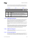
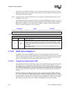
The end/error in FIFO (EIF) flag is set within status register 0 whenever one or more of the tag bits
(8 – 10) are set within any of the bottom eight entries of the receive FIFO and is cleared when no
error bits are set in the bottom eight entries of the FIFO. When EIF is set, an interrupt is generated
and receive FIFO DMA requests are disabled so that the user can manually empty the FIFO,
always checking the end-of-frame, CRC error, and overrun error flags in status register 1 first
before removing each data value from the FIFO. After each entry is removed, the user should
check the EIF bit to see if any set end or error tag remains, and repeat the procedure until all set
tags are flushed from the bottom eight entries of the FIFO. Once EIF is cleared, servicing of the
receive FIFO by the DMA controller is automatically reenabled.
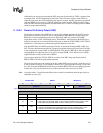
When HSDR is written, the topmost entry of the 8-bit transmit FIFO is accessed. After a write, data
is automatically transferred down to the lowest location within the transmit FIFO, which does not
already contain valid data. Data is removed from the bottom of the FIFO one piece at a time by the
transmit logic, encoded using the 4PPM modulation technique, loaded into the transmit serial
shifter, then serially shifted out onto the TXD2 pin.
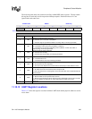
Note: A question mark (?) signifies that the Reset value of that bit is undefined when the processor has
completed its reset cycle.